| Feb 03, 2022 |
A revolutionary customizable fabrication platform for electronic skins (w/videos) |
| (Nanowerk Spotlight) For years, thin-film electronics have shown their superior performance over conventional electronic devices in many applications. Consequently, the demand for thin-film devices is continuing to grow at a rapid pace. |
| Thin-film electronics are mostly attached to something, for instance as flexible sensors to skin, but the specific characteristics of the target location cannot always be determined. In this case, conventional simulation technology loses its benefit as a tool to optimize device performance and decrease prototyping cost. |
| Conventional skin electronics are fixed designs that lack consideration for the individual characteristics of the wearer as well as the ability to actively adapt to various user specifications. |
| In order to manage different sensor specifications and body impedances, design adjustments are inevitable during fabrication of these devices. Unfortunately, conventional fabrication methods can be costly and time consuming, even when making small modifications to existing circuit designs. |
| To address this issue, researchers at Seoul National University have developed a real-time fabrication platform that can adapt to arbitrary environments by freely drawing or erasing paths in a printed circuit. The system utilizes a laser-based process in which concentrated light sinters or ablates metallic nanoparticles on a flexible ultra-thin substrate. |
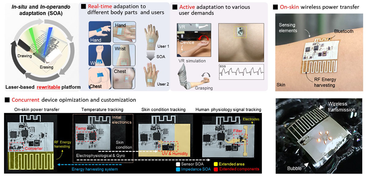 |
| Illustration of the impedance and sensor in situ and in operando adaptation (SOA). The device is actively adapted to the various user demands and corresponding attachment locations through impedance and sensor SOA. (Image: Applied Nano and Thermal Science Lab, Seoul National University) (click on image to enlarge) |
| This research is described in a paper in Advanced Functional Materials ("Evolvable Skin Electronics by In Situ and In Operando Adaptation"). This revolutionary customizable electronic fabrication platform allows simultaneous evolvable design modification and addition of new functionality to original skin electronics while they are in operation. |
| "Our findings enable us to easily draw and erase electronics in wearables in a real-time manner according to a user's needs," Professor Seung Hwan Ko from the Applied Nano and Thermal Science (ANTS) Lab at Seoul National University, tells Nanowerk. "We found that controlling the source and the power of the laser light could anneal metal nanoparticles to create conductive paths, and also to selectively erase existing circuits. In addition, we can stack several layers and selectively create interconnections between them." |
| The researchers call this process in situ and in operando adaptation, or SOA. SOA allows the instant adaptation of electronic skin devices for arbitrary users and placement. For instance, the team demonstrated that an electronic skin device originally designed for monitoring temperature can be extended to include UV and humidity sensors. Moreover, wireless power transmission of the device is enabled while attached on user’s skin through real-time antenna modification. This is crucial since the electromagnetic properties vary from user to user and body part to body part. |
| For instance, the team demonstrated that an electronic skin device originally designed for monitoring temperature can be extended to include UV and humidity sensors. Moreover, wireless power transmission of the device, while attached on human skin, was enabled through real-time antenna modification. |
| In situ and in operando adaptation (SOA) is based on a rewriting scheme with two main features: 1) additive manufacturing by visible wavelength laser sintering of metal nanoparticles, and 2) subtractive manufacturing through ultraviolet laser ablation. Each laser source selectively converts silver nanoparticles into electrically connected layers or removes existing electrical patterns. (Video: Applied Nano and Thermal Science Lab, Seoul National University) |
| They describe in their paper how this novel platform enables immediate response to various user specifications, offering concurrent customization for various wearable and wireless applications. The system can be applied in various potential applications with wireless/battery-less operation, such as skin condition tracking, human physiological measurements, and VR application. |
| The system is even sufficient to operate an electronic circuit remotely. The researchers successfully operated the circuit to control a vehicle in up to 50 cm distance from the transmitter by using a long dipole antenna. |
| A dipole antenna system attached on a paper-based controller used to remotely control a vehicle with a battery-less controller. (Video: Applied Nano and Thermal Science Lab, Seoul National University) |
| The SOA process can be repeated as many times as required to add or remove functionalities such as skin condition monitoring, human physiological measurements, motion tracking, and so on. |
| "Since SOA is conducted by lasers, we need to understand some characteristics of the laser systems," Ko explains. "There might be some alternative settings, but we exploited continuous laser with a wavelength of 532nm (green) for circuit drawing and pulse laser with a wavelength of 355nm (ultraviolet) for circuit erasing. Theoretically, both lasers can replace each other, yet the speed and quality of the processes are significantly different." |
| The waveform of laser against time has a crucial effect on heat dissipation at the target. The pulsed laser provides high energy during a very short time, hence the heat provided to the spot does not have enough time to dissipate. As a result, the narrow but highly heated region evaporates. |
| Whereas the continuous laser provides constant power to the target, hence the generated heat at the spot has a better chance to dissipate to the neighboring region than is the case with the pulsed laser. As a consequence, the metal nanoparticles melt rather than evaporate and the melted metal becomes a metal film that is formed as the laser passes by. The wavelength of the continuous laser is related to the absorbance of the material, and 532nm is the wavelength that the metal nanoparticles absorb the most. |
| As the team points out, at the initial stage of the process, the erasing process is the trickiest part of SOA as it could erase the uppermost circuit layer but also could cause damage to the lower circuit layer. Since the insulation layer has only a thickness of 2∼3 µm, the operating condition of the erasing laser have to be finely tuned. |
| Though low-power conditions may prevent damage, they inevitably result in a slow process, which would restrict practical usage of the SOA. By using colorless polyimide as an ultra-thin substrate, the low absorbance of this insulating material mitigated the damage on the insulation layer, allowing reasonable erasing speed. |
| The developed sensor is used to control a virtual hand in real-time. (Video: Applied Nano and Thermal Science Lab, Seoul National University) |
| In a next step, the team is planning to develop an automatic optimizing algorithm for analog SOA. |
| "Existing simulation tools for analog systems support parametric study on sets of geometrical properties – such as length, width, the number of some patterns – which determine the performance of an analog system," Ko notes. "Our current SOA process conducts parametric studies only for a single parameter such as the length of an antenna. We therefore need a new algorithm that determines which parameters to change among many for a given state and that estimates the optimal state during fabrication process." |
| He adds that this approach has enough potential as a next-generation optimization tool for various analog systems including antennas and metamaterials. |
 By
Michael
Berger
– Michael is author of four books by the Royal Society of Chemistry:
Nano-Society: Pushing the Boundaries of Technology (2009),
Nanotechnology: The Future is Tiny (2016),
Nanoengineering: The Skills and Tools Making Technology Invisible (2019), and
Waste not! How Nanotechnologies Can Increase Efficiencies Throughout Society (2025)
Copyright ©
Nanowerk LLC
By
Michael
Berger
– Michael is author of four books by the Royal Society of Chemistry:
Nano-Society: Pushing the Boundaries of Technology (2009),
Nanotechnology: The Future is Tiny (2016),
Nanoengineering: The Skills and Tools Making Technology Invisible (2019), and
Waste not! How Nanotechnologies Can Increase Efficiencies Throughout Society (2025)
Copyright ©
Nanowerk LLC
|

Become a Spotlight guest author! Join our large and growing group of guest contributors. Have you just published a scientific paper or have other exciting developments to share with the nanotechnology community? Here is how to publish on nanowerk.com. |
