| Feb 17, 2022 |
Using DNA to make nanoelectronics |
| (Nanowerk Spotlight) DNA, the fundamental building block of our genetic makeup, is being widely used by nanotechnology researchers to create artificial rationally designed nanostructures for diverse applications in biology, chemistry, and physics. DNA could be particularly useful for the design of electronics and DNA-based computing because it self-assembles, it self-replicates and it can adopt various states and conformations (read more in our previous Nanowerk Spotlight "The ongoing development of DNA nanotechnology"). |
| To realize the full potential of DNA nanotechnology in nanoelectronics applications requires addressing a number of scientific and engineering challenges: how to create and manipulate DNA nanostructures? How to use them for surface patterning and integrating heterogeneous materials at the nanoscale? And how to use these processes to produce electronic devices at lower cost and with better performance? |
| These topics are the focus of a recent review in Advanced Functional Materials ("DNA-Based Nanofabrication for Nanoelectronics"). |
| The authors begin with an introduction of the fabrication of DNA nanostructures, followed by reviewing the principles of using DNA nanostructures to engineer various functional interfaces that were further used to fabricate nanoelectronic devices. The review concludes with a brief discussion of the challenges and research opportunities of DNA-based nanofabrication. |
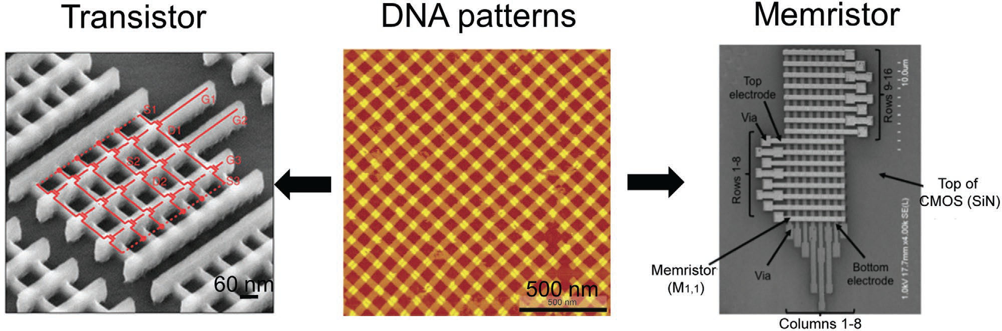 |
| Similarity between nanoelectronics (Fin-FET, left) and memristors (16 x 8 memristor array, right) with DNA nanopatterns (lattice, middle). (Reproduced with permission by Wiley-VCH Verlag) |
| As illustrated in the figure above, DNA nanostructures can easily be assembled into various patterns that resemble nanoelectronic structures. The field effect transistor (FET) for example has three key components: the conductive wiring for the source, drain, and gate electrodes; the semiconductor channel where charge transport is modulated; and the gate dielectric enabling capacitive modulation of the semiconductor channel. Individual DNA nanostructures can integrate heterogeneous materials with nanometer-scale resolution, which could serve as the template for self-assembling FET-like structures. |
| As another example illustrated above, DNA nanostructure lattices can be made with tens of nanometer of periodicity and complex unit cell patterns. These structures can potentially be used as template for patterning arrays of memristors, which can be fabricated from simple crossbar structures. |
| In reviewing how researchers use DNA nanostructures to build functional electronic interfaces, the authors address in great detail the topics of DNA-templated doping, DNA-templated conductive nanostructures, DNA-templated dielectric and semiconductor nanostructures, DNA-enabled integration of nanomaterials, and DNA-based lithography. |
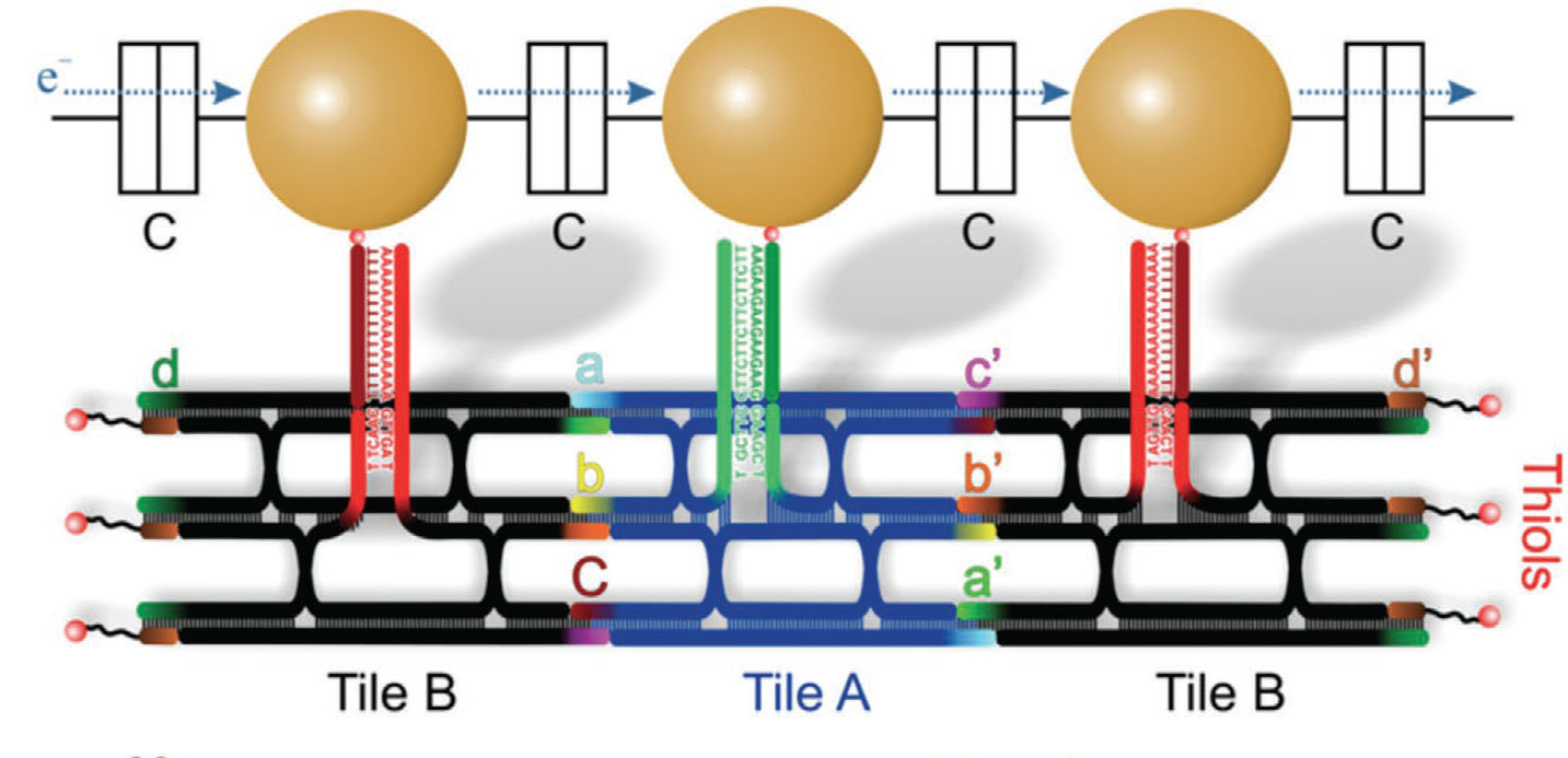 |
| DNA-assisted fabrication of single electron transistors. A) Schematic illustration of DNA-gold complex. The spacing between the sticky ends is 14 nm. Gold nanoparticles are attached to these sticky ends and serve as a chain of isolated islands for single electron transistors. C is the capacitance of the tunnel junctions formed between the gold nanoparticles by a tiny gap filled with single strand DNA and air. (Reproduced with permission by Wiley-VCH Verlag) |
| Having the ability to fine-tune their structure and functionalization makes DNA nanostructures not only a good template for electronics fabrication, but a unique platform for sensing, in particular single-molecular detection. Here, the authors address the potential of using DNA nanostructures to build biomedical sensors that have single molecular resolution, high sensitivity and specificity, as well as greatly reduced production cost. |
| Combined with other technologies such as machine learning, DNA-based platforms could further advance the development of DNA/protein sequencing, data storage, and omics analysis. |
| Although there has been tremendous progress made in the development of DNA nanotechnology and applying them to the fabrication of electronics, photonics, and sensing architectures, there are still major challenges facing the translation of technology into commercial products. Some of the key bottleneck issues that the authors single out for future research endeavors are: |
| The stability of DNA nanostructures. The chemical and physical stability of DNA nanostructures often become the limiting factor in research work. Given the scarcity of research aiming at understanding and improving their stability, much more effort is needed to make DNA nanostructures a robust template for their intended applications, especially in a dry state. |
| Placement of DNA nanostructures. The ability to precisely align DNA nanostructures over large areas and do so with low defect rates is critical for large-scale integration of electronic and photonic devices. While self-assembly can form DNA superlattices, the precision of such assembly is far from what is required by the semiconductor industry. Currently, the most promising solution to this problem is guided assembly, where the deposition of DNA nanostructure is directed and facilitated by nanoscale surface features made by lithography techniques. |
| Defects. On the individual DNA nanostructure level, are multiple types of defects can occur, such as imperfection in the molecular structure of DNA base, imperfections in base paring, defects in functionalization, and missing or misplaced DNA strands. For superlattices of DNA nanostructure, including the ones produced by guided assembly, the defects are mostly imperfections (missing structure, mis-orientation) within the assembly. Reducing defects, both in an individual DNA nanostructure and in a superlattice of DNA nanostructures, is critical to many applications, especially in the fabrication of integrated circuits and photonic devices. |
 By
Michael
Berger
– Michael is author of four books by the Royal Society of Chemistry:
Nano-Society: Pushing the Boundaries of Technology (2009),
Nanotechnology: The Future is Tiny (2016),
Nanoengineering: The Skills and Tools Making Technology Invisible (2019), and
Waste not! How Nanotechnologies Can Increase Efficiencies Throughout Society (2025)
Copyright ©
Nanowerk LLC
By
Michael
Berger
– Michael is author of four books by the Royal Society of Chemistry:
Nano-Society: Pushing the Boundaries of Technology (2009),
Nanotechnology: The Future is Tiny (2016),
Nanoengineering: The Skills and Tools Making Technology Invisible (2019), and
Waste not! How Nanotechnologies Can Increase Efficiencies Throughout Society (2025)
Copyright ©
Nanowerk LLC
|

Become a Spotlight guest author! Join our large and growing group of guest contributors. Have you just published a scientific paper or have other exciting developments to share with the nanotechnology community? Here is how to publish on nanowerk.com. |
