| Mar 24, 2022 |
A cost-effective and lithography-free method for printing optical metasurfaces |
| (Nanowerk Spotlight) Optical metasurfaces are sub-wavelength nanopatterned layers that interact strongly with light, thus dramatically altering the light properties over a sub-wavelength thickness. They offer a fundamentally new method of light manipulation based on scattering from resonant nanostructures rather than conventional refraction and propagation, thus offering efficient phase, polarization, and emission control. |
| Optical metasurfaces have been employed for the design and fabrication of ultra-thin optical elements and systems with abilities that surpass the performance of conventional diffractive optical elements. They enable a range of novel applications such as skin cloaks or flat metalenses and more efficient holograms. |
| Metasurfaces can be fabricated using standard lithography and nanoimprinting methods. However, these methods are suitable only for smaller areas as the structural complexity of optical metasurfaces poses a challenge to their upscaling and large-volume applications. |
| Researchers have now addressed this issue with a lithography-free method for printing optical metasurfaces. They do this by employing an optical cavity formed by a multilayer structure of ultra-thin metal and dielectric coatings and with a critical coupling condition, where the absorption of the optical cavity at the in-resonance writing frequency is near-perfect. |
| This work has been reported in Nano Letters ("Resonant Laser Printing of Optical Metasurfaces"). |
| "Conventional laser processing technologies rely on the high energy density in a focused beam derived from a pulsed laser, in combination with ultrashort femto- to picoseconds pulses to spatially confine the laser-induced heating," Prof. Xiaolong Zhu from the State Key Laboratory of Precision Spectroscopy at East China Normal University in Shanghai, explains to Nanowerk. "For instance, ultrafast femtosecond lasers have recently been introduced for post-processing as-prepared metasurfaces, where the near-infrared femtosecond pulses are typically not in resonance with resonant features of the plasmonic or dielectric nanoantennas resonating at the visible." |
| "In contrast" he continues, "resonant laser printing, applied in our current work, utilizes resonant features with enhanced light confinement in plasmonics or high-index-material resonators." |
| With resonant laser printing the team achieve metasurfaces for structural colors (where the colors are solely a result of the interaction of the nanostructured surface and light), optical holograms, and diffractive optical elements, with an energy consumption of less than 1 nanojoule and a print time down to 1 nanosecond per dot. |
| As the 'paper' for laser printing, the researchers used an ultra-thin film consisting of a lossless dielectric (TiO2), embedded between a perfect aluminum conductor and a thin, semitransparent, lossy gold metal film. This multi-layer film is easy to fabricate and cost effective for upscaling and lager-area fabrication. |
| They note that the nanoscale structures made on this Al-TiO2-gold film are robust and typically could last longer than most inks or pigments. |
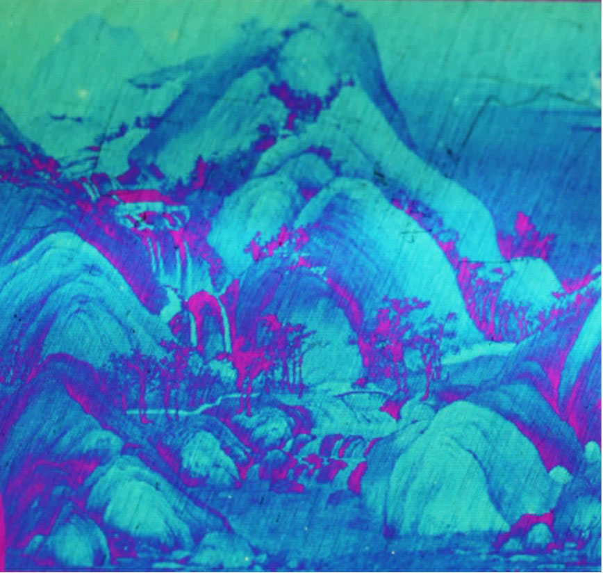 |
| The laser structure color printing of a section of "A Thousand Miles of Rivers and Mountains" created by the researchers is 4cm x 4cm, with a resolution of more than 100 000 dpi (dots per inch), which is by far the highest laser color printing resolution in the world. The original work by Wang Ximeng of the Northern Song Dynasty is exhibited in the Palace Museum in Beijing. (Image: Xiaolong Zhu, East China Normal University) |
| The performance of this ink-free laser color printing with a resolution of more than 100 000 dpi by far exceeds the output of conventional laser printers or inkjet printers that usually have a printing resolution of less than 1200 dpi. |
| "Another breakthrough proposed in our paper is the discovery that the surface structure of a thin-film optical microcavity can not only adjust the amplitude of incident light, that is, the different structural colors, but also adjust the phase of incident light wave and the corresponding wavefront structure," Zhu points out. "Near the critical coupling point, the optical metasurface structure can realize the drastic change and wide-range regulation of the phase of the incident light even in the case of external field perturbation." |
| This principle can be used to realize the large-scale preparation of a surface structure that can produce optical holograms. With this ultra-high resolution of resonance laser printing it becomes possible to print large-scale optical phase information within a limited area. This is demonstrated in the image below where 16 million pixels are printed on a 2mm x 2mm area depicting a holographic butterfly. |
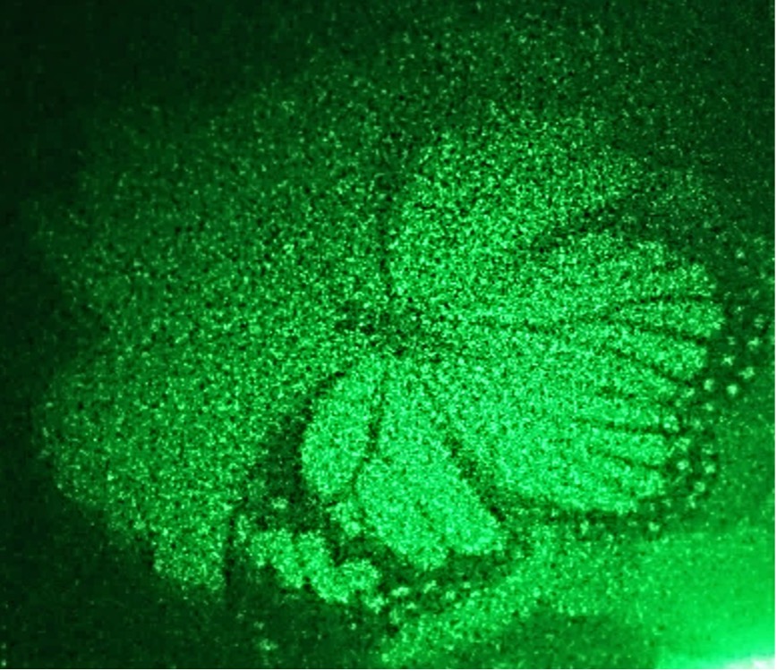 |
| Holographic butterfly printed on a 2mm x 2mm area with 16 million pixels. (Image: Xiaolong Zhu, East China Normal University) |
| This work shows the reliability, upscalability, and subwavelength resolution of laser printing of metasurfaces, which may pave the way for the industrial applications of optical metasurfaces in color printing, or flat optical elements such as metalenses and waveplates. |
| "By introducing the interfacial phase shifts, our approach with free-form, self-organized nanostructures enables the realization of metasurface holograms and flat optical elements with unprecedented capabilities," Zhu concludes. "Hologram movies can be completely re-envisioned with our solution, by replacing expensive, time-consuming, and sophisticated electron-beam nanolithography procedures." |
 By
Michael
Berger
– Michael is author of four books by the Royal Society of Chemistry:
Nano-Society: Pushing the Boundaries of Technology (2009),
Nanotechnology: The Future is Tiny (2016),
Nanoengineering: The Skills and Tools Making Technology Invisible (2019), and
Waste not! How Nanotechnologies Can Increase Efficiencies Throughout Society (2025)
Copyright ©
Nanowerk LLC
By
Michael
Berger
– Michael is author of four books by the Royal Society of Chemistry:
Nano-Society: Pushing the Boundaries of Technology (2009),
Nanotechnology: The Future is Tiny (2016),
Nanoengineering: The Skills and Tools Making Technology Invisible (2019), and
Waste not! How Nanotechnologies Can Increase Efficiencies Throughout Society (2025)
Copyright ©
Nanowerk LLC
|

Become a Spotlight guest author! Join our large and growing group of guest contributors. Have you just published a scientific paper or have other exciting developments to share with the nanotechnology community? Here is how to publish on nanowerk.com. |
