| Sep 27, 2022 |
MXene with its X factor may help downscaling 2D transistors |
| (Nanowerk Spotlight) On December 26, 1947, the two physicists Walter Brattain and John Bardeen, officially demonstrated the first point-contact transistor at Bell Labs. Later, in January 1948, William Shockley, one of the pioneers of semiconductor device physics, presented the first junction transistor, which marked the practical beginning of the age of transistors. Technology kept improving over time, and the transistor, one of the most important inventions in history, notably revolutionized the human lifestyle. During the years 2022 and 2023, we are celebrating the 75th anniversary of the transistor's invention. |
| Although this point-contact, three-terminal semiconductor device was initially conceived as an analog amplifier, its technology was adapted as a digital switch over time. Transistors have evolved in terms of current control mechanism (from bipolar junction transistor to various forms of field effect transistors) and size (sub-millimeter to deca-nanometer). Downscaling like this, aided by the remarkable sophistication of semiconductor technology, has allowed us to pack millions of transistors in a unit area of silicon wafer. The operation of most of the equipment we use every day – smartphones, electric vehicles, computers, televisions, etc. – is based on the transistors' properties and the integrated circuits built with them. |
| However, it has been predicted that a fundamental down-scaling limit for silicon technology will be reached within the next few years. Therefore, it has become a necessity for the semiconductor industry to look for other alternatives. After the discovery of graphene in 2004, various atomically thin layered materials – also known as 2D materials – have attracted attention for transistor applications. Because of their inherent "thin-ness," they promise to outperform bulk silicon in technology downscaling. |
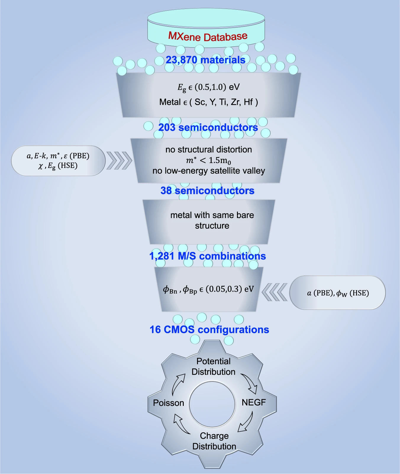 |
| High-throughput computational pipeline to screen suitable MXene materials for transistor applications and assess their electrical properties. (Image courtesy of the researchers) |
| After the first revelation of a monolayer molybdenum disulfide (MoS2) based metal-oxide-field-effect transistor in 2011, many MoS2 devices based on transistor architecture – phototransistors, memory devices, and sensors – have been studied, and extraordinary properties like excellent mobility, ON/OFF ratio, and sensitivity of these devices have been reported. |
| Moreover, integrated circuits built upon 2D transistors have been demonstrated for diverse applications: simple logic inverter, 1-bit microprocessor, operational amplifier, and neuromorphic computation. Despite such intense efforts, the high contact resistance at the interface between the 2D material and the external metallic circuits has appeared as the key obstacle for realizing high-performance transistors with sub-decananometer channel lengths. |
| Approaches like metal work function engineering, 2D/2D interfacing, graphene/hBN interlayer insertion, and surface charge transfer doping have been attempted to mitigate the effect of high contact resistance at the interface. However, most of them lack scalability. |
| Meanwhile, dozens of 2D materials have been explored experimentally (and hundreds of them computationally), MXenes have been neglected for MOS transistor applications. MXenes, a group of non-van der Waals 2D materials first reported in 2011, have gathered attention due to their fascinating mechanical and electronic properties. |
| In this work (npj Computational Materials, "High-throughput design of functional-engineered MXene transistors with low-resistive contacts"), we show how MXenes' rich chemistry can be used to create doping-free 2D transistors with intrinsically low resistive contacts while maintaining balance mode operation. |
| MXenes' bare structure is usually metallic; however, with a suitable functional termination, it can become a semiconductor or a metal with a different work function. In our work, we exploit this unique property of MXene to propose a Schottky barrier transistor, which can be implemented with a bare MXene by converting it to a semiconductor in the channel region with strategic functionalization. |
| To validate our concept, we have developed a high-throughput computational pipeline to identify 16 such CMOS configurations by screening materials from an extensive MXene database (hosting more than 23 000 materials). After that, we have predicted their performance with an in-house GPU-based self-consistent quantum transport simulator. |
| Performance of these devices has been found to meet the international roadmap for devices and systems (IRDS) requirements for several benchmark metrics. The proposed balanced-mode, functional-engineered MXene transistors may lead to a realistic solution for the sub-deca nanometer technology scaling by enabling doping-free intrinsically low contact resistance. |
| By Professor Santanu Mahapatra, Nano-Scale Device Research Laboratory, Department of Electronic Systems Engineering, Indian Institute of Science Bangalore |

Become a Spotlight guest author! Join our large and growing group of guest contributors. Have you just published a scientific paper or have other exciting developments to share with the nanotechnology community? Here is how to publish on nanowerk.com. |
