| Nov 01, 2022 |
Electrical gating of the charge-density-wave quantum phases opens up innovative electronic applications |
| (Nanowerk Spotlight) The charge-density-wave (CDW) phase is a macroscopic quantum state consisting of a periodic modulation of the electronic charge density accompanied by a periodic distortion of the atomic lattice. |
| The early work on CDW effects revealed many spectacular phenomena: oscillating electric current for constant voltages, giant dielectric response, and multi-stable conducting states. Recent years witnessed a rebirth of the field of CDW materials and devices, partially driven by an interest in layered quasi-2D van der Waals materials where CDW phases can manifest themselves at room temperature. |
| The 1T polymorph of TaS2 is one of the prominent members of the quasi-2D van der Waals materials that reveal several CDW phase transitions in the form of resistivity changes and hysteresis. These transitions can be induced by temperature, electric current, and light. However, despite numerous attempts, the electrical gating of the CDW phase, which is needed for many practical applications, remained elusive. |
| In recent work, a research team led by Distinguished Professor Alexander A. Balandin, Department of Electrical and Computer Engineering, University of California, Riverside (UCR), reported electrical gating of the CDW quantum phases in h-BN/1T-TaS2 devices in the journal ACS Nano ("Electrical Gating of the Charge-Density-Wave Phases in Two-Dimensional h-BN/1T-TaS2 Devices"). |
| Maedeh Taheri, the first author of the paper who built and tested the devices, is a Ph.D. candidate in Balandin’s Nano-Device Laboratory and the Phonon Optimized Engineered Materials (POEM) Center. |
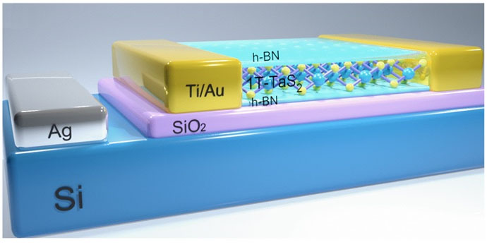 |
| Figure 1: Schematic of the 1T-TaS2 heterostructure devices encapsulated in h-BN layers fabricated at the University of California. In 1T-TaS2 crystal, the Ta atoms are depicted in blue while sulfurs are in yellow colors. (Image: Maedeh Taheri and Alexander A. Balandin) |
| "Gating of CDW phases enhances the functionality of the CDW devices and creates potential opportunities for applications in electronics, for example in memory," explains Balandin. "The great thing about this material is that it can undergo charge-density-wave quantum phase transitions near and above room temperature." |
| It was reported in prior works that 1T-TaS2 CDW devices have the potential for application in oscillators, detectors, and radiation-hard electronics. The devices reported to date were two-terminal, with the resistive state and hysteresis controlled by the source-drain current. |
| These CDW devices utilized the hysteresis window and negative feedback for their operation rather than the on-off ratio in the resistance change. The demonstrated electrical gating of the CDW quantum condensate was achieved in three-terminal devices (see Figure 1), similar in their design to field-effect transistors. |
| "The main difficulty of electrical gating of the CDW phases and currents in this van der Waals material is associated with the fact that different CDW phases still have a rather high concentration of electrons," says Balandin. |
| The team achieved electrical gating by using an interesting approach. They pass a small electric current in the device channel, creating a slight local Joule heating, which softens the commensurate CDW domains and makes them more susceptible to the electric gating potential (Figure 2). |
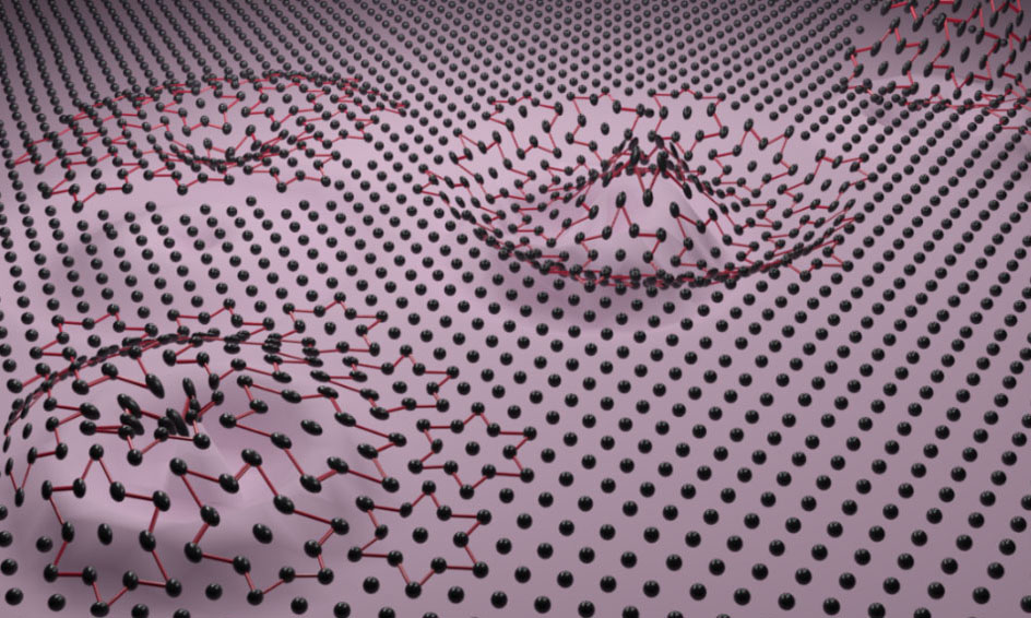 |
| Figure 2: Illustration of the charge-density-wave domains subjected to the electrical potential. The black dots represent atoms. The atoms of the domains are arranged in certain structures, characteristic of the CDW phase. (Image: Maedeh Taheri) |
| The CDW domain switching can be potentially utilized in non-volatile memory applications, particularly if the channel area and thickness are downscaled to the 100-nm-scale or below, allowing for control of individual CDW domains that exist up to the temperature of ∼350 K. |
| One can find an analogy in the heat-assisted magnetic recording (HAMR), an existing magnetic storage technology, which increases the amount of data that can be stored on a magnetic device by temporarily heating the disk material during writing, which makes it much more receptive to magnetic effects and allows writing the info to much smaller regions. |
| In the team's proof-of-concept demonstrations, the application of the electric gate switched the material phase between the nearly commensurate CDW and incommensurate CDW phases (Figure 3). |
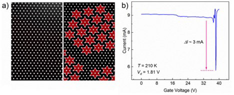 |
| Figure 3: (a) Illustration of the incommensurate CDW and nearly-commensurate CDW phases. (b) Current as a function of the source-drain voltage at two fixed gate biases. In this device, the transition between two CDW phases, depicted with red and blue dots, occurs at a voltage close to Vd = 1.83 V. (Image: Maedeh Taheri and Alexander A. Balandin) |
| "In our approach, we pass a small source-drain current, which produces small heating and 'softens' the CDW domains, and then we apply gate bias to electrically switch the C-CDW domains," explains Balandin. |
| Another potentially promising feature of the demonstrated gating of the CDW domains is the small source-drain voltages, currents, and power involved. The gate bias was relatively large due to the thick SiO2 layers used in the proof-of-concept experiments, but it can be reduced significantly in the actual technology. |
| The small power required for 'softening and switching the CDW domains in quasi-2D CDW materials can give them an advantage as compared to many “conventional” resistive switching materials and devices. |
| "The key will be downscaling the size of the CDW devices to allow for an individual CDW domain switching with the gate," Balandin concludes. |
| Provided by the University of California, Riverside |

Become a Spotlight guest author! Join our large and growing group of guest contributors. Have you just published a scientific paper or have other exciting developments to share with the nanotechnology community? Here is how to publish on nanowerk.com. |
