| Jul 10, 2023 |
Unleashing the future of printed magnetoelectronics with roll-to-roll processing of magnetic multilayers |
| (Nanowerk Spotlight) The concept of Magnetoresistance, with a special focus on Giant Magnetoresistance (GMR), has been a driving force in technological advancements. The inception of this concept can be traced back to the pivotal works of Albert Fert and Peter Grunberg in the 1980s. Their ground-breaking research on thin metallic systems initiated a multitude of applications in various sectors, such as the automotive and biomedical industries contactless sensors in aviation and space industry, magnetic compasses. Despite the vast potential of the GMR effect, the transition of its use and integration in printed electronics has been challenged by obstacles arising from wafer scale manufacturing and costly semiconductor processes. Furthermore, the low yield of GMR material due to traditional deposition methods has been a significant hindrance to progress. |
| However, in the past decade, we've seen a rise in the focus on flexible, stretchable, and printable technologies as an alternate route, owing to their additive manufacturing possibilities. Unlike subtractive processes such as photolithography, etching, and deposition techniques, additive manufacturing is less harmful to the environment and uses fewer raw materials. Such technologies have been instrumental in the breakthrough of intelligent and smart polymer-based flexible and printable electronics. |
| What has made this possible is the use of thin polymeric substrates, which have made electronics more accessible with their low fabrication costs, mechanical flexibility, and larger working areas. The potential for high throughput roll-to-roll (R2R) and sheet-to-sheet (S2S) systems have further increased the applicability of these technologies. Advancements in functional materials and fabrication processes have resulted in new building blocks for flexible and printable electronic circuits, such as interconnects, transistors, and sensors. |
| The success of printed flexible devices, such as gas, temperature, strain, and magnetic sensors, has been due to their potential applications in diverse fields including soft robotics, electronic skins, wearable electronics, smart textiles, contactless human-machine interfaces, and future bio-integrated consumer electronics. Their adaptability to various surface geometries has facilitated their use in areas like liquid level monitors and flexible position sensors. |
| Nevertheless, the potential of magnetosensitive inks is still limited by the yield of GMR material. Current fabrication methods are confined by the size of the carrier substrate, producing only a few milligrams of material, which is insufficient for large-scale industrial applications. |
| "To bring GMR materials into mainstream printed technology, we need a significant increase in GMR material yield, ideally by 2 to 4 orders of magnitude," Dr. Preeti Gupta, a Postdoctoral Research Fellow at the Leibniz Institute for Solid State and Materials Research in Dresden, Germany, tells Nanowerk. "However, this involves substantial challenges, including acquiring larger equipment and improved process control, especially considering the production of GMR base material, which is typically prepared in semiconductor grade facilities." |
| In response to these challenges, the solution may lie in a large-scale deposition technique for GMR thin-film on a flexible substrate. A candidate that holds considerable promise is the roll-to-roll coating technique. Unlike traditional semiconductor facilities, R2R methods are able to accommodate much larger areas, thereby playing a pivotal role in enabling cost-effective production of thin-film coatings on a variety of materials, including polymers, metals, and flexible glasses. |
| Gupta is first and corresponding author of a paper in Advanced Materials Technologies ("Large Scale Exchange Coupled Metallic Multilayers by Roll-to-Roll (R2R) Process for Advanced Printed Magnetoelectronics"), that presents the first fully roll-to-roll processed flexible GMR thin-films with large-area deposition approach providing high-yield of magnetoresistive material. |
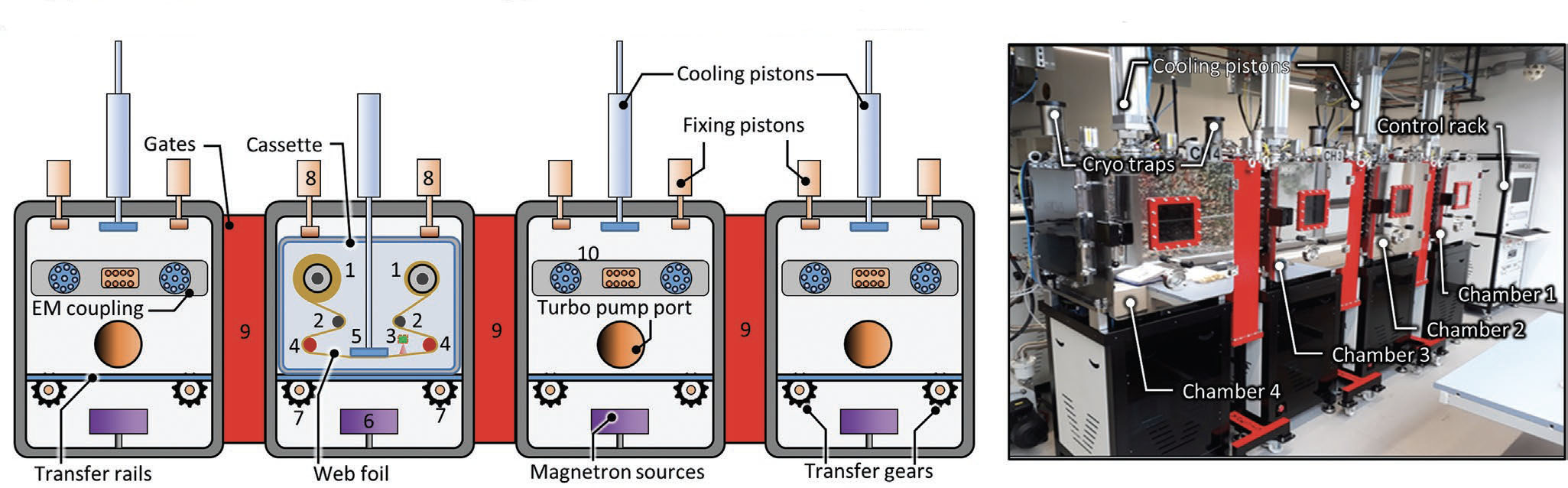 |
| The modular roll-to-roll deposition system with a movable cassette. Left: Schematic of the deposition system consisting of four deposition chamber modules, which are isolated from each other with gates. Cassette inside the chamber with the roll-to-roll foil transfer system consisting of 1) web foil rolls, 2) idle rolls, 3) bar code scanner, 4) tension rolls. Each chamber is equipped with 5) cooling piston, 6) deposition source, 7) transfer gears and rails, 8) cassette fixing pistons, and 9) chamber isolation gates. Right: Photograph of the actual system. (Reprinted and adapted with permission from Wiley VCH Verlag) |
| In this work, the team, led by Dr. Daniil Karnaushenko, devised a bespoke R2R thin-film magnetron sputtering system specifically to deposit precise metal multilayers under high vacuum conditions. This pioneering approach facilitates the production of GMR material on standard polymeric films, a feat that has not been achieved before. |
| "This breakthrough allows for continuous manufacturing on 100 m long plastic sheets but not limited to, making these materials suitable for use in a wide range of hybrid magnetoelectronic devices," she notes. "The system also achieved a remarkable improvement in sensitivity, setting a new record for practical applications. Additionally, the conversion of these magnetic thin films into special ink enables the printing of high-performance magnetic sensors." |
| This printing method is not only cost-effective but also allows for seamless integration with other printed electronics. It pushes the boundaries of large-scale manufacturing, improves the sensitivity of magneto-sensitive systems, and promotes the integration of magnetic sensors with printed electronics. |
| These advancements have the potential to impact various fields, including electronics, sensors, and wearable devices, by enabling the production of more efficient, cost-effective, and versatile electronic components. |
| The R2R process brings with it a plethora of benefits, including reduced material costs, a decrease in capital and energy expenditure, and a lowering of production-related labor costs. These advantages render the R2R process particularly attractive for industrial scale applications. Moreover, the R2R process significantly boosts reliability and reproducibility, which are critical factors for large-scale production. This is achieved by offering control over the end product quality and specifications. |
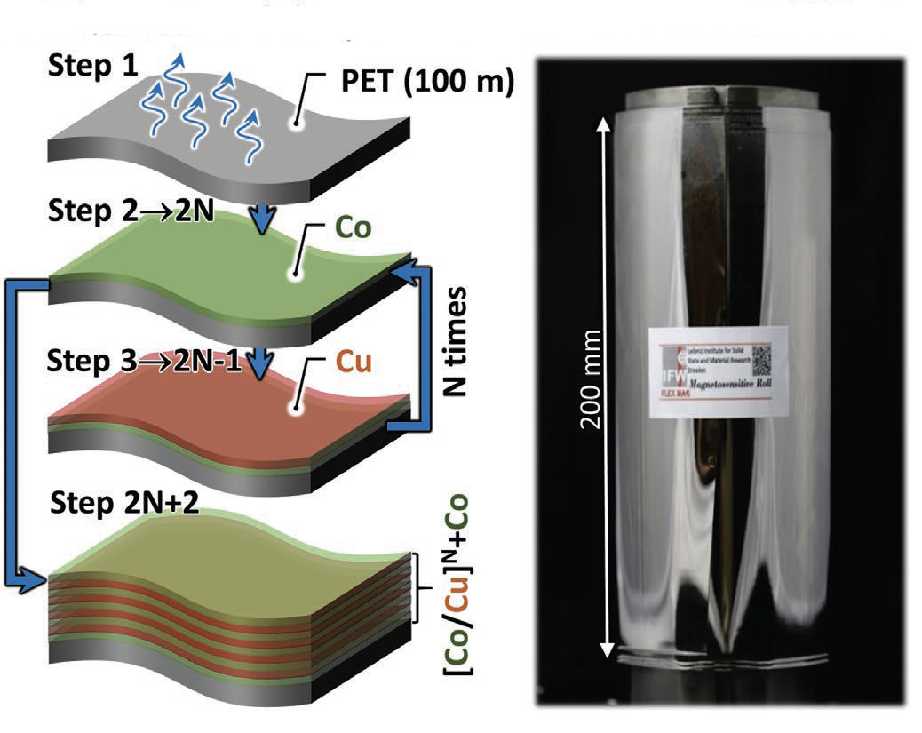 |
| Giant magnetoresistive thin-films on polyethylene terephthalate web. Left: Schematic representation of Co/Cu multilayer deposition process on the PET web by R2R magnetron sputtering. Right: Magnetosensitive R2R deposited GMR multilayer on 0.2 × 100 m2 PET web (Reprinted and adapted with permission from Wiley VCH Verlag) |
| This new R2R process represents a sea change in terms of its operational efficiency. It has enabled an approximately 10,000-fold increase in the functional deposited area of multilayers fabricated in a single run, while concurrently achieving a 150-fold reduction in processing time as compared to conventional wafer scale coating approaches. |
| In tandem with these efficiencies, the team developed an optimized magnetosensitive ink formulation process to ensure consistent batch production of GMR ink cartridges. This includes optimizing the viscosity and other properties of the ink to ensure optimal performance and compatibility with printing tools and processes. |
| "One of the most intriguing aspects of our work is the significant increase in the functional area of deposited GMR thin films," Gupta points out. "In a single run, we achieved a staggering 10 000 times larger area compared to conventional coating methods. To put it into perspective, a mere 100 meter long GMR film deposited on a flexible PET substrate is equivalent to 637 eight-inch wafers! Not only have we revolutionized the scale of production, but we have also dramatically reduced the processing time. By streamlining the manufacturing process, we have achieved a remarkable 150-fold decrease in processing time compared to traditional approaches. This breakthrough not only saves valuable time but also significantly cuts down on costs." |
| Dr. Oliver G Schmidt, one of the co-authors and a visionary scientist and renowned expert in the field, anticipates that his research team's innovative efforts will streamline the incorporation of cost-effective magnetic sensors into electronics across various sectors, thereby expanding the technology's accessibility. |
| The success of this approach and high yield of magnetosensitive powder has led to the potential for printable magnetoresistive sensors. These sensors can be embedded into flexible circuits, smart textiles, and other electronic devices with magnetic sensing capabilities, revolutionizing sectors like healthcare, wearable technology, and IoT devices. |
| Moreover, the versatility of the R2R process extends beyond magnetoelectronics, enabling its application to various functional materials and thereby opening new avenues for large-scale manufacturing. This could have implications in areas such as energy storage and biomedical applications, requiring precise and large-area production. The potential for innovative advancements is immense, offering the prospect of a future where magnetoelectronic systems are an integral part of everyday life. Printable magnetoresistive sensors could give rise to a new generation of intelligent, adaptable electronic devices, reflecting our evolving needs. |
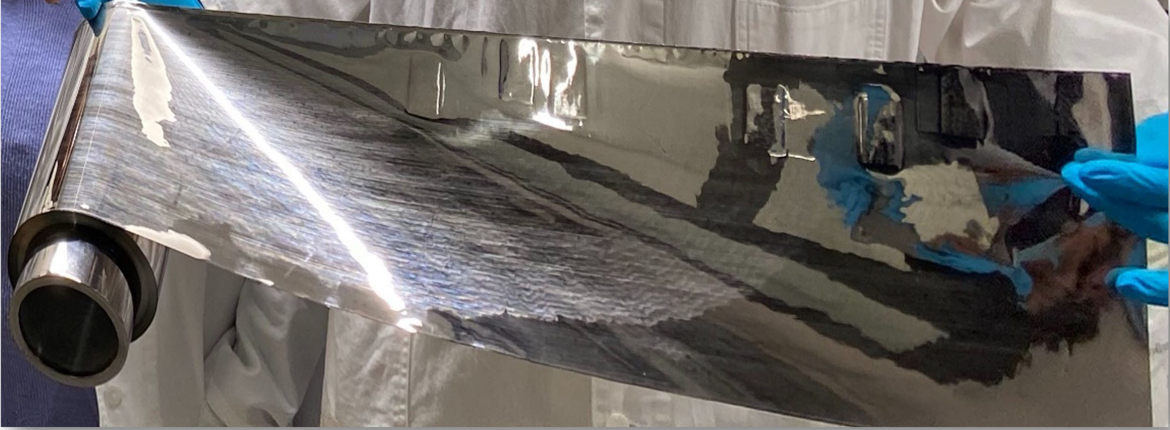 |
| First Large scale R2R sputtered 100 m GMR thin film with Co/Cu multilayers. (Image courtesy of the researchers) |
| "In the upcoming phase of our research, we are prioritizing performance evaluation, batch scale processing, and exploring printing techniques and substrates," Gupta describes the team's next steps. "Our plan includes thorough testing of 10,000 printed magnetic sensors to assess their resistance and GMR ratio for better efficiency. We aim to elevate the production of magnetosensitive powder and its ink formulation while increasing our focus on the versatility of our magnetosensitive ink by testing different printing techniques and substrates. Our overarching goal is to advance the field of magnetoelectronics and catalyze its widespread adoption across industries such as automotive, healthcare, and biomedical sectors." |
| "As we look ahead, the field of magnetosensitive materials research holds fascinating prospects," she concludes. "We stand on the precipice of revolutionizing large-scale production processes, achieving unprecedented sensor performance, and seamlessly fusing with state-of-the-art technologies. Yet, it's critical to acknowledge that we face daunting challenges in terms of materials development, manufacturing scalability, performance reliability, and the complexity of integration. Surmounting these obstacles is the key to unlocking the transformative potential of printed magnetic sensors across a multitude of industries and applications. The future of magnetoelectronics is vibrant and filled with promise, and we remain committed to turning this promise into reality." |
 By
Michael
Berger
– Michael is author of four books by the Royal Society of Chemistry:
Nano-Society: Pushing the Boundaries of Technology (2009),
Nanotechnology: The Future is Tiny (2016),
Nanoengineering: The Skills and Tools Making Technology Invisible (2019), and
Waste not! How Nanotechnologies Can Increase Efficiencies Throughout Society (2025)
Copyright ©
Nanowerk LLC
By
Michael
Berger
– Michael is author of four books by the Royal Society of Chemistry:
Nano-Society: Pushing the Boundaries of Technology (2009),
Nanotechnology: The Future is Tiny (2016),
Nanoengineering: The Skills and Tools Making Technology Invisible (2019), and
Waste not! How Nanotechnologies Can Increase Efficiencies Throughout Society (2025)
Copyright ©
Nanowerk LLC
|

Become a Spotlight guest author! Join our large and growing group of guest contributors. Have you just published a scientific paper or have other exciting developments to share with the nanotechnology community? Here is how to publish on nanowerk.com. |
