| Nov 09, 2023 |
The Synthescope vision for future nanomaterial synthesis |
| (Nanowerk Spotlight) Scientists are developing new ways to observe and direct the construction of materials at the smallest scales. Recent advances in scanning transmission electron microscopes (STEMs) have opened up the possibility of manipulating individual atoms to build precise nanostructures. |
| A new perspective article in Advanced Materials ("The Synthescope: A Vision for Combining Synthesis with Atomic Fabrication") proposes enhancements to STEMs that could enable researchers to synthesize materials atom-by-atom while observing the process in real time. With such capabilities, scientists could gain unprecedented insights into nanoscale growth mechanisms with the potential to revolutionize fields like microelectronics and catalysis. |
| For decades, STEMs have been indispensable for imaging materials down to the level of atoms. These powerful microscopes focus a beam of electrons onto a thin sample, detecting signals that reveal the sample's atomic structure. But electron beams can also modify samples by knocking atoms out of place. Historically this beam damage was seen as an undesirable side effect, but recently scientists have learned to exploit it for the controlled rearrangement of atoms. |
| With improved control, the authors have previously envisioned STEMs evolving into true "atomic forges" that build custom nanostructures through atom manipulation (see Nature, "Fire up the atom forge"). But current capabilities remain limited. The main strategy uses the beam to sputter atoms off a source material onto the sample surface, where they sometimes bind to vacancy sites created by beam damage. This cycle of beam sputtering and damage enables patterning but lacks the efficiency and flexibility of a true synthesis approach. |
| To achieve atom-by-atom growth, the authors propose enhancing STEMs with local material sources such as evaporative filaments or laser ablation targets. This would allow continuous deposition synchronized to beam-induced reactions on the sample surface. With separate control over the supply rate and surface reactivity, scientists could tune synthesis conditions to promote the controlled build-up of structures atom-by-atom. The electron beam could potentially even guide the growth by steering atoms to desired sites. |
| Meanwhile, new specimen holders would enable simultaneous imaging, property measurements, and atomic fabrication. Chips with integrated heater circuits could control surface diffusion effects, while membranes transparent to the electron beam would provide views of the atomic action. This combination of synthesis capabilities and real-time feedback is dubbed the “synthescope” by the researchers. |
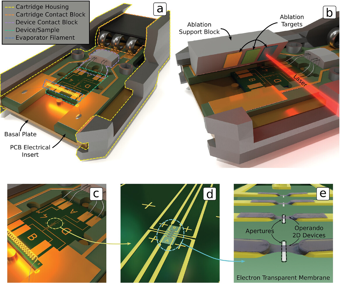 |
| Concept drawings illustrating simple approaches toward the development of the synthescope approach. a) An evaporator filament is incorporated on the end of a printed circuit board (PCB) that overhangs the device/sample. Electrical operation is facilitated through the use of existing electrical contacting holders. b) A strategy for laser ablation deposition is illustrated. This approach would require cutting an access notch in the holder cartridge and installation of a commercially available laser. Multiple ablation targets could be used to facilitate switching source materials. c) Magnified view of (a), showing electrical integration with a previously developed wafer-scale chip design. d) Electrical traces converge at the center of the chip where the operational devices are supported on an electron-transparent membrane (e) to be compatible with STEM imaging. (Reprinted with permission by Wiley-VCH Verlag) (click on image to enlarge) |
| With a synthescope, scientists could directly observe processes like nucleation, growth of crystals or nanoparticles, and incorporation of dopants into materials. By dynamically tuning parameters like temperature and deposition rate, they could optimize processes or switch material compositions on the fly. Such insights could prove invaluable for rational design of materials and devices. |
| For instance, the precise placement of just a few dopant atoms in key areas can greatly enhance the properties of 2D materials. And locating single atoms at the active sites of a catalyst can strongly influence its performance. |
| Realizing this vision will require further advances, from cleaner vacuum environments to redesigned hardware. But proof-of-principle experiments have already shown the feasibility of integrating localized material sources with STEMs. With focused research and development, synthescopes could open up a new paradigm for materials science within the next decade. |
| In their Perspective, the authors lay out a trajectory for progress in this emerging field. Early milestones like molecule-by-molecule deposition have already been achieved using STEMs' finely focused electron beams. But replicating traditional electron beam-induced deposition at the atomic scale presents challenges due to contamination issues. An alternate approach that uses beam damage to create reactive sites for atom incorporation shows more promise. Recent demonstrations of this technique achieved dopant patterning in 2D materials. |
| Ongoing improvements will require decoupling the atom supply from the imaging electron beam. The proposed synthescope could meet this need with integrated material sources. Controlled introduction of vaporized or laser-ablated atoms during beam patterning would enable precise atom-by-atom growth. Further developing strategies like feedback-controlled synthesis and multi-element deposition will maximize these tools' potential. |
| Guided by an unprecedented view into nanoscale synthesis, scientists will explore the vast possibilities for constructing matter from the atom up. With the synthetic power and analytical capabilities envisioned for synthescopes, researchers could uncover new nanoscale growth mechanisms and phenomena. These insights can then inform the design of more effective large-scale synthesis techniques. |
| In this way, synthescopes have the potential to revolutionize our fundamental understanding of materials formation while accelerating the development of atomically engineered structures for applications ranging from electronics to energy conversion and storage. |
 By
Michael
Berger
– Michael is author of four books by the Royal Society of Chemistry:
Nano-Society: Pushing the Boundaries of Technology (2009),
Nanotechnology: The Future is Tiny (2016),
Nanoengineering: The Skills and Tools Making Technology Invisible (2019), and
Waste not! How Nanotechnologies Can Increase Efficiencies Throughout Society (2025)
Copyright ©
Nanowerk LLC
By
Michael
Berger
– Michael is author of four books by the Royal Society of Chemistry:
Nano-Society: Pushing the Boundaries of Technology (2009),
Nanotechnology: The Future is Tiny (2016),
Nanoengineering: The Skills and Tools Making Technology Invisible (2019), and
Waste not! How Nanotechnologies Can Increase Efficiencies Throughout Society (2025)
Copyright ©
Nanowerk LLC
|

Become a Spotlight guest author! Join our large and growing group of guest contributors. Have you just published a scientific paper or have other exciting developments to share with the nanotechnology community? Here is how to publish on nanowerk.com. |
