| Nov 22, 2023 |
3D Nanoprinting technique enables tunable plasmonic structures |
| (Nanowerk Spotlight) Plasmonic nanoparticles have drawn considerable interest owing to their unique optical properties and increasing use in commercial applications ranging from sensors to optoelectronics. The geometry and arrangement of these tiny structures determine the strength and frequency of localized surface plasmon resonances – the means by which they concentrate and enhance light. Controlling these aspects is therefore critical for reproducible, optimized performance. |
| Most research has focused on planar configurations made using techniques with limited 3D capabilities. However, recent work demonstrates the immense possibilities of tunable 3D nanoparticles. Manipulating plasmons along vertical and horizontal axes simultaneously may strengthen plasmonic hot spots and enable as-yet unrealized devices. But reliably fabricating intricate 3D nanoparticles has proven extremely challenging for existing methods. |
| Now researchers at Graz University of Technology have shown that a flexible technique called focused electron beam induced deposition (FEBID) can directly 3D print gold nanostructures with customizable, predictable plasmonic responses. Unlike planar fabrication, the additive FEBID process works on nearly any substrate or surface geometry. This unique capacity promises broad applicability from augmented spectroscopy to quantum optics. |
| Their findings have been published in Advanced Functional Materials ("Spectral Tuning of Plasmonic Activity in 3D Nanostructures via High-Precision Nano-Printing"). |
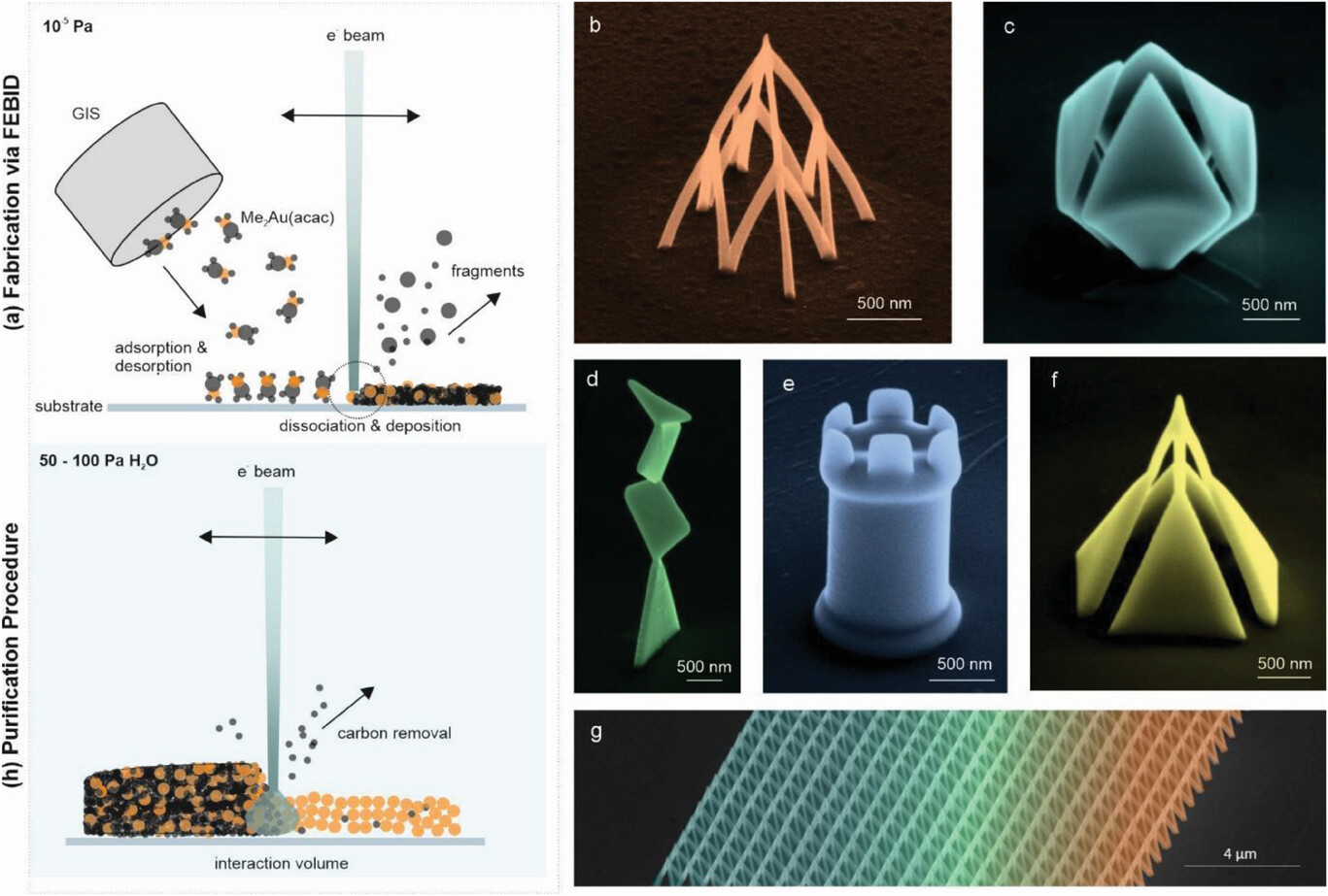 |
| Fabrication, purification, and 3D possibilities. a) A gas injection system (GIS) injects preheated precursor molecules in gaseous states (Me2(acac)Au(III) in this study) in close proximity to the substrate, where they adsorb, diffuse and, if not dissociated, eventually desorb again. Upon interaction with a focused electron beam, local dissociation leads to immobilization of the respective metal, which forms the intended deposit. As a result of incomplete ligand cleavage not only Au atoms (orange spheres) but also carbonaceous fragments (grey spheres) are co-deposited, which is why FEBID structures naturally contain high amounts of carbon. The whole fabrication procedure is typically performed at 21±1 °C and 10−5 Pa. b–g) depicts 3D nano-printing design possibilities, ranging from meshed objects (b) over sheet-like, semi-closed (c, d) toward closed (e) and mixed architectures (f). Also, scalability is provided, as shown in (g) by a tetrapod array, to generate micrometer-sized assemblies for individual applications. To remove the carbon, scheme (h) illustrates a suitable purification process, which takes place in a low-pressure H2O atmosphere ranging between 50–100 Pa at 21±1 °C. Using again the focused electron beam leads to the local removal of carbon, leaving nominally pure, polycrystalline gold nanostructures with a volume loss of up to two thirds. Depending on the height of the nanostructure, the beam conditions have to be adapted such that the interaction volume can cover the whole structure volume. (Reprinted with permission by Wiley-VCH Verlag) |
| After printing and purifying simple nanowires, the team combined scanning transmission electron microscopy with electron energy loss spectroscopy (STEM-EELS). This technique visualizes the plasmonic activity across the nanostructures, verifying strong enhancement at targeted locations determined by geometry. Simulating the nanowires with customized dimensions agreed closely with experiments, confirming predictable tuning. |
| The researchers then printed complex 3D antennas over 1 µm tall topped by ∼10 nm radii – the smallest controllably realized to date. Despite the intricate shape, simulations again matched experiments. By adjusting models systematically, the peak intensity, frequency, and density of distinct plasmon modes shift in well-behaved ways. This further demonstrates reliable predictability and spectral tunability. |
| For example, making antennas taller redshifts and intensifies specific resonances. Shorter antennas produce fewer plasmon peaks per wavelength range, while longer ones squeeze more into a desired band. Such relationships govern where light concentration occurs and at which energies. |
| With this upfront simulation capability proven, designing any arbitrary nanostructure with application-specific optical properties becomes straightforward and efficient. Instead of exhaustive trial and error, the guided approach reduces experiments to targeted verification. The 3D nanoprinting flexibility also allows placing tuned plasmonic elements on finished device components like sensors. |
| Compared to previous works, these findings enable precise vertical and lateral mode engineering in complex geometries. Coupled interactions between assemblies of 3D nanoparticles—now manufacturable on-demand—could better confine light beyond the diffraction limit or improve quantum emitters. Other applications may emerge as more research utilizes this new freedom to devise tunable 3D nanoplasmonic architectures. |
 By
Michael
Berger
– Michael is author of four books by the Royal Society of Chemistry:
Nano-Society: Pushing the Boundaries of Technology (2009),
Nanotechnology: The Future is Tiny (2016),
Nanoengineering: The Skills and Tools Making Technology Invisible (2019), and
Waste not! How Nanotechnologies Can Increase Efficiencies Throughout Society (2025)
Copyright ©
Nanowerk LLC
By
Michael
Berger
– Michael is author of four books by the Royal Society of Chemistry:
Nano-Society: Pushing the Boundaries of Technology (2009),
Nanotechnology: The Future is Tiny (2016),
Nanoengineering: The Skills and Tools Making Technology Invisible (2019), and
Waste not! How Nanotechnologies Can Increase Efficiencies Throughout Society (2025)
Copyright ©
Nanowerk LLC
|

Become a Spotlight guest author! Join our large and growing group of guest contributors. Have you just published a scientific paper or have other exciting developments to share with the nanotechnology community? Here is how to publish on nanowerk.com. |
