| Posted: Dec 17, 2014 |
Discovery opens door for radical reduction in energy consumed by digital devices
|
|
(Nanowerk News) An article in Nature Materials ("Negative capacitance in a ferroelectric capacitor") describes the first direct observation of a long-hypothesized but elusive phenomenon called “negative capacitance.” The work describes a unique reaction of electrical charge to applied voltage in a ferroelectric material that could open the door to a radical reduction in the power consumed by transistors and the devices containing them.
|
|
Capacitance is the ability of a material to store an electrical charge. Ordinary capacitors—found in virtually all electronic devices—store charge as a voltage is applied to them. The new phenomenon has a paradoxical response: when the applied voltage is increased, the charge goes down. Hence its name, negative capacitance.
|
|
“This property, if successfully integrated into transistors, could reduce the amount of power they consume by at least an order of magnitude, and perhaps much more,” says the paper’s lead author Asif Khan. That would lead to longer-lasting cell phone batteries, less energy-consumptive computers of all types, and, perhaps even more importantly, could extend by decades the trend toward faster, smaller processors that has defined the digital revolution since its birth.
|
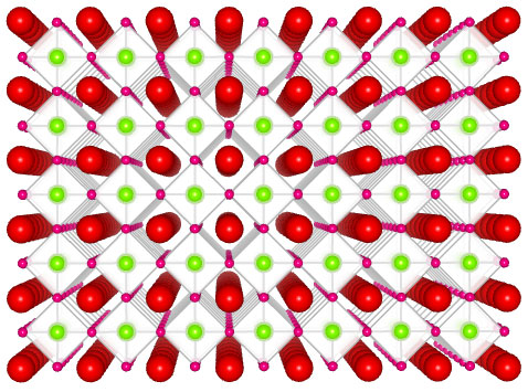 |
| The atomic structure of a ferroelectric material exhibits the so-called “negative capacitance” effect. If successfully built into transistors, it could drastically reduce the electricity needed to run computer processors and other transistor-dependent devices. (Illustration: Suraj S. Cheema)
|
|
Without a major breakthrough of this sort, the trend toward miniaturization and increased function is threatened by the physical demands of transistors operating at a nano scale. Even though the tiny switches can be made ever smaller, the amount of power they need to be turned on and off can be reduced only so much. That limit is defined by what is known as the Boltzmann distribution of electrons—often called the Boltzmann Tyranny. Because they must be fed an irreducible amount of electricity, ultra-small transistors that are packed too tightly cannot dissipate the heat they generate to avoid self-immolation.
|
|
In another decade or so, engineers will exhaust options for packing more computing power into ever tinier spaces, a consequence viewed with dread by device manufacturers, sensor developers, and a public addicted to ever smaller and more powerful devices.
|
|
The new research, conducted at UC Berkeley under the leadership of CITRIS researcher and associate professor of electrical engineering and computer sciences Sayeef Salahuddin, provides a possible way to overcome the Boltzmann Tyranny. It relies on the ability of certain materials to store energy intrinsically and then exploit it to amplify the input voltage. This could, in effect, potentially “trick” a transistor into thinking that it has received the minimum amount of voltage necessary to operate. The result: less electricity is needed to turn a transistor on or off, which is the universal operation at the core of all computer processing.
|
|
The material used to achieve negative capacitance falls in a class of crystalline materials called ferroelectrics, which was first described in the 1940s. These materials have long been researched for memory applications and commercial storage technologies. Ferroelectrics are also popular materials for frequency control circuits and many microelectromechanical systems (MEMS) applications. However, the possibility of using these materials for energy efficient transistors was first proposed by Salahuddin in 2008, right before he joined Berkeley as an assistant professor.
|
|
Over the past six years, Khan—one of Salahuddin’s first graduate students at Berkeley—has used pulse lasers to grow many kinds of ferroelectric materials and has devised and revised ingenious ways to test for their negative capacitance.
|
|
In addition to transforming the way transistors work, negative capacitance could also potentially be used to develop high-density memory storage devices, super capacitors, coil-free oscillators and resonators, and for harvesting energy from the environment.
|
|
Exploiting the negative capacitance of ferroelectrics is one in a list of strategies for reducing the per-joule cost of storing a single bit of information, says UC Berkeley professor of materials science, engineering, and physics Ramamoorthy Ramesh, another of the paper’s authors. Ramesh’s decades of seminal work on ferroelectric materials and device structures for manipulating them underlies the group’s findings.
|
|
“We have just launched a program called the attojoule-per-bit program. It is an effort to reduce the total energy consumed for manipulating a bit to one attojoule (10-18),” says Ramesh. To achieve that kind of per-bit energy consumption, we need to take advantage of all possible pathways. The negative capacitance of ferroelectrics is going to be a very important one,” he says.
|
|
This work was enabled by access to CITRIS’s Marvell Nanofabrication Laboratory, a research facility on the UC Berkeley campus that specifically encourages the exploration of new materials and processes. One of the most advanced academic nanofabrication labs of its type in the world, the NanoLab is the birthplace of other game-changing technologies, such as the three-dimensional FinFET transistor that has led the way to scaling far beyond the limits of ordinary transistors. “Today,” says professor Ming Wu, Marvell NanoLab Faculty Director, “every single transistor built for next-generation microprocessors or computers is FinFET.”
|
|
“CITRIS’s Marvell NanoLab has state-of-the-art equipment for making semiconductor devices and integrated circuits,” says Wu. “But we take these tools and capabilities and apply them to materials that are so new that industry fabrication labs would not touch them. New materials like these negative capacitance ferroelectrics are not only welcome here, they are actively encouraged.”
|
|
“The next step,” says Salahuddin, “is to try to make actual transistors such that they can exploit the new phenomenon, We need to make sure they are compatible with silicon processing, that they are manufacturable, and that the measurement techniques we’ve now proven in principle are practical and scalable.”
|