| Posted: Mar 02, 2015 |
Ultrathin layers of black phosphorus improve optical communication
|
|
(Nanowerk News) Phosphorus, a highly reactive element commonly found in match heads, tracer bullets, and fertilizers, can be turned into a stable crystalline form known as black phosphorus. In a new study, researchers from the University of Minnesota used an ultrathin black phosphorus film--only 20 layers of atoms--to demonstrate high-speed data communication on nanoscale optical circuits.
|
|
The devices showed vast improvement in efficiency over comparable devices using the earlier "wonder material" graphene.
|
|
The work by University of Minnesota Department of Electrical and Computer Engineering Professors Mo Li and Steven Koester and graduate students Nathan Youngblood and Che Chen was published today in Nature Photonics ("Waveguide-integrated black phosphorus photodetector with high responsivity and low dark current").
|
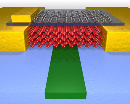 |
| This illustration shows the high performance photodetector which uses few layer black phosphorus (red atoms) to sense light in the waveguide (green material). Graphene (gray atoms) is also used to tune the performance. (University of Minnesota, College of Science and Engineering)
|
|
As consumers demand electronic devices that are faster and smaller, electronics makers cram more processor cores on a single chip, but getting all those processors to communicate with each other has been a key challenge for researchers. The goal is to find materials that will allow high-speed, on-chip communication using light.
|
|
While the existence of black phosphorus has been known for more than a century, only in the past year has its potential as a semiconductor been realized. Due to its unique properties, black phosphorus can be used to detect light very effectively, making it desirable for optical applications. For the first time, the University of Minnesota team created intricate optical circuits in silicon and then laid thin flakes of black phosphorus over these structures using facilities at the University's Minnesota Nano Center.
|
|
"After the discovery of graphene, new two-dimensional materials continue to emerge with novel optoelectronic properties," said Professor Li, who led the research team. "Because these materials are two-dimensional, it makes perfect sense to place them on chips with flat optical integrated circuits to allow maximal interaction with light and optimally utilize their novel properties."
|
|
The University of Minnesota team demonstrated that the performance of the black phosphorus photodetectors even rivals that of comparable devices made of germanium--considered the gold standard in on-chip photodetection. Germanium, however, is difficult to grow on silicon optical circuits, while black phosphorus and other two-dimensional materials can be grown separately and transferred onto any material, making them much more versatile.
|
|
The team also showed that the devices could be used for real-world applications by sending high-speed optical data over fibers and recovering it using the black phosphorus photodetectors. The group demonstrated data speeds up to three billion bits per second, which is equivalent to downloading a typical HD movie in about 30 seconds.
|
|
"Even though we have already demonstrated high speed operation with our devices, we expect higher transfer rates through further optimization," said Nathan Youngblood, the lead author of the study. "Since we are the first to demonstrate a high speed photodetector using black phosphorus, more work still needs to be done to determine the theoretical limits for a fully optimized device."
|
|
Bridging the gap
|
|
While black phosphorus has much in common with graphene--another two-dimensional material--the materials have significant differences, the most important of which is the existence of an energy gap, often referred to as a "band gap."
|
|
Materials with a band gap, known as "semiconductors," are a special group of materials that only conduct electricity when the electrons in that material absorb enough energy for them to "jump" the band gap. This energy can be provided through heat, light, and other means.
|
|
While graphene has proven useful for a wide variety of applications, its main limitation is its lack of a band gap. This means that graphene always conducts a significant amount of electricity, and this "leakage" makes graphene devices inefficient. In essence, the device is "on" and leaking electricity all the time.
|
|
Black phosphorus, on the other hand, has a widely-tunable band gap that varies depending on how many layers are stacked together. This means that black phosphorus can be tuned to absorb light in the visible range but also in the infrared. This large degree of tunability makes black phosphorus a unique material that can be used for a wide range of applications--from chemical sensing to optical communication.
|
|
Additionally, black phosphorus is a so-called "direct-band" semiconductor, meaning it has the potential to efficiently convert electrical signals back into light. Combined with its high performance photodetection abilities, black phosphorus could also be used to generate light in an optical circuit, making it a one-stop solution for on-chip optical communication.
|
|
"It is really exciting to think of a single material that can be used to send and receive data optically and is not limited to a specific substrate or wavelength," Youngblood said. "This could have huge potential for high-speed communication between CPU cores which is a bottleneck in computing industry right now."
|
|
Fast growing potential
|
|
The past several years have seen a flurry of two-dimensional material discoveries, first with graphene, more recently with transition metal dichalcogenides (TMDs) such as molybdenum disulphide (MoS2), and now black phosphorus. All of the previous two-dimensional materials have serious trade offs, but black phosphorus provides the "best of both worlds" with a tunable band gap and high-speed capability.
|
|
"Black phosphorus is an extremely versatile material," said Professor Steven Koester, who contributed to the project. "It makes great transistors and photodetectors, and has the potential for light emission and other novel devices, making it an ideal platform for a new type of adaptable electronics technology."
|