| Posted: Mar 04, 2015 |
Using supercomputers to design nanoelectronics components
|
|
(Nanowerk News) A relentless global effort to shrink transistors has made computers continually faster, cheaper and smaller over the last 40 years. This effort has enabled chipmakers to double the number of transistors on a chip roughly every 18 months--a trend referred to as Moore's Law. In the process, the U.S. semiconductor industry has become one of the nation's largest export industries, valued at more than $65 billion a year.
|
|
The foundation of this industry's success has been the development of progressively more capable chips. However, according to the International Technology Roadmap for Semiconductors (ITRS), which identifies technological challenges and needs for the semiconductor industry over the next 15 years, signs point to a disruption in these long-running trends.
|
|
Transistor size will continue to decrease for a decade, reaching approximately 5 nanometers long and 1 nanometer (or about 5 atoms) wide in its critical active region. Beyond that point, what happens is harder to predict.
|
|
At this nanoscale, new phenomena take precedence over those that hold sway in the macro-world. Quantum effects such as tunneling and atomistic disorder dominate the characteristics of these nanoscale devices. Fundamental questions about how various materials and configurations behave at this scale need to be answered.
|
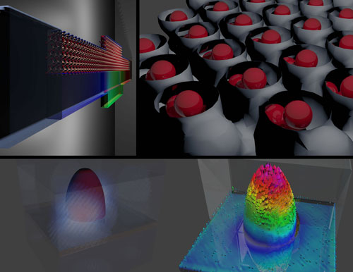 |
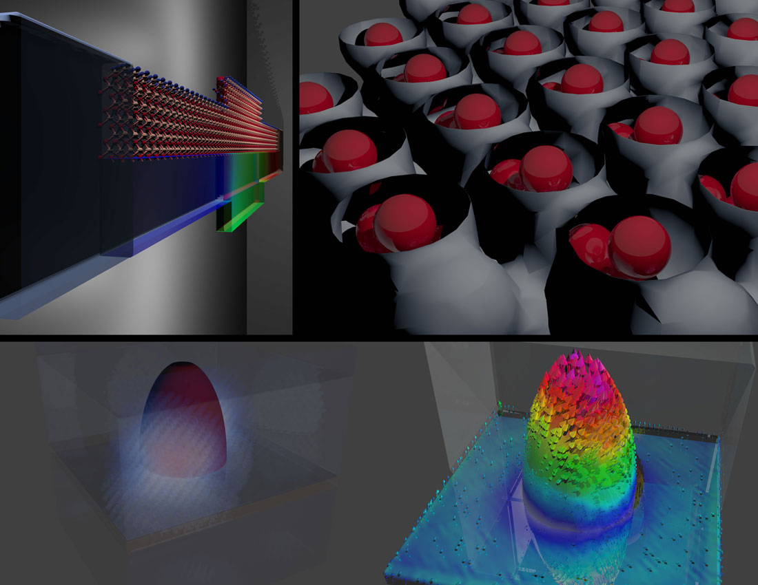
| Visualizations of future nano-transistors, clockwise starting at upper left: a) The picture shows the organization of the atoms in an Ultra Thin Body (UTB) transistor and the amount of electric potential along the transistor. b) This is a visualization of the organization of the atoms in a pure material. Each atom (in red) is surrounded by a grey shell, representing the interaction field of each atom. c) Quantum dots are nanoscale particles, with diameters approximately 1000 times smaller than the diameter of human hair. This image shows the magnitude of the strain forces on the surface of a quantum dot's core. d) A quantum dot's core can have different shapes and composition. Both of these factors affect the energy levels inside a quantum dot. This figure in light blue represents the intensity of an energy level inside a quantum dot with a conic core (in red). (Image: Institute for Nanoelectronic Modeling). (click on image to enlarge)
|
|
"Further improvements in these dimensions will come only through detailed and optimized device design and better integration," said Gerhard Klimeck, a professor of electrical and computer engineering at Purdue University and director of the Network for Computational Nanotechnology there.
|
|
It is at the scale of atoms guided by nanoscale and quantum interactions that Klimeck works. He leads a team that developed one of the primary software tools used by academics, semiconductor companies and students to predict the future behavior of nanoscale transistors.
|
|
Called NEMO5 (the fifth edition of the NanoElectronics MOdeling Tools), the software simulates the multiscale, multiphysics phenomena that occur when an electric charge passes through a few-atoms-wide transistor. In doing so, NEMO helps researchers design future generations of nanoelectronics, including transistors and quantum dots, even before they can be physically produced, and predicts device performances and phenomena that researchers otherwise couldn't explore.
|
|
"There are no computer-aided design tools that can model these devices in an atomistic sense," Klimeck said. "All the standard semiconductor device design tools that are out there assume that matter is smooth and continuous and ignore the existence of atoms."
|
|
But atoms do exist, and their behavior needs to be taken into account when designing devices only a few atoms across.
|
|
"What we're building is an engineering tool that will be used in the understanding and design of devices that are at the end of Moore's Law," Klimeck noted.
|
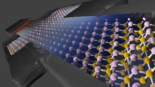 |
| This picture represents an internal representation of an Ultra Thin Body (UTB) transistor. The position of the atoms and their chemical bonds are presented along with the amount of electric potential in the transistor. The electrical potential can be seen as colored surfaces overlapped with the structure. (Image: Institute for Nanoelectronic Modeling). (click on image to enlarge)
|
|
With a Petascale Computing Resource Allocation award from the National Science Foundation, Klimeck's group is using the Blue Waters supercomputer at the National Center for Supercomputing Applications to study the limits of current semiconductor technologies and the possibilities of future ones. Blue Waters is one of the world's most powerful machines for simulation, modeling and data analysis.
|
|
Mehdi Salmani and SungGeun Kim, formerly Ph.D. students in Klimeck's group, used Blue Waters to model various devices and configurations for the International Technology Roadmap for Semiconductors. They explored whether the ever-smaller devices that are projected to be available in the next 15 years are physically feasible. They also determined what impact quantum effects like scattering and confinement might have on performance as devices shrink down to critical thresholds.
|
|
Simulations by Klimeck's team found important deviations in the characteristics of devices as they are scaled down, raising questions about future device designs. Their results were included in the ITRS roadmap in 2014 and are helping to guide the direction of many of the largest semiconductor companies in their planning and future research and development.
|
|
Klimeck's team also used Blue Waters to explore alternative materials that may replace silicon in future devices. These include indium arsenide and indium antimonide, as well as exotic materials such as graphene, carbon nanotubes and topological insulators for quantum spin computers.
|
|
Results of their simulations were published in Nature Nanotechnology ("Spin blockade and exchange in Coulomb-confined silicon double quantum dots") in April 2014 and in Applied Physics Letters ("Transistor roadmap projection using predictive full-band atomistic modeling") in August 2014.
|
|
NEMO5, and its predecessors OMEN and NEMO3D, power nine applications on nanoHUB, a website that hosts a growing collection of simulation programs for modeling nanoscale phenomena. Since they were released almost 15 years ago, more than 19,000 researchers have run over 367,000 simulations using the NEMO family of tools. NEMO and OMEN have been used in 381 classes at institutions around the world and have been cited in 84 papers in the scientific literature.
|
|
"The public availability of such tools supports rapid innovation and accelerates the adoption of disruptive technologies into tomorrow's high-tech devices," said Keith Roper, who oversees the Network for Computational Nanotechnology program in the Engineering directorate at NSF.
|
|
Combining high-performance modeling tools like NEMO5 with a high-performance modeling system like Blue Waters is allowing Klimeck and hundreds of other researchers to ask questions and find solutions far beyond those that they could address in the past.
|
|
"The typical problem we need to handle has maybe 100,000 to a million atoms," Klimeck said. "Ten years ago people would have told me that isn't solvable. You can't get a computer that's big enough. Now that the petascale Blue Waters system is available, we can solve these kinds of problems and help design semiconductors that will allow for continued technological growth."
|