| Posted: Mar 30, 2015 |
Physicists report technology with potential for sub-micron optical switches
|
|
(Nanowerk News) A team that includes Rutgers University and National Institute of Standards and Technology scientists believes that a technology it is reporting this week in Nature Photonics ("Compact nanomechanical plasmonic phase modulators") could result in optical switches with sub-square-micron footprints, potentially allowing densely packed switching fabrics on a chip.
|
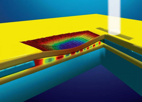 |
| Surface plasmons are propagating electronic oscillations localized to metal-insulator (e.g. gold-air) interfaces. Gap plasmons (GPs) arise when two such interfaces are separated by a narrow gap across the insulator layer, transversely confining the electromagnetic energy in an MIM (metal-insulator-metal) waveguide. In this illustration, a free-space excitation laser (vertical light on the right) couples to GPs (alternating red/blue light) in a gold/air/gold nanofabricated waveguide. A grating is used to match the laser light momentum with to a GP. The GP propagates through the waveguide under free-floating micro-beams in the top gold layer (color coded to show depth). When the beams are electrically actuated towards the bottom gold layer, the effective refractive index of the waveguide increases under the beams, phase-retarding the GP. (Image: Brian Dennis, Rutgers University)
|
|
These dimensions contrast with established optical switching technologies based on other technologies, such as MEMS, lithium niobate, and silicon and electro-optic polymer plasmonic technologies, that have active elements in scales up to hundreds of microns.
|
|
The scientists have shown that an optical signal can be modulated in a 200 nanometer-high waveguide. The signal's phase is modulated as it passes through an air gap between two gold layers, when a force generated by the device slightly deforms the top gold layer.
|
|
The scientists propose that when one of these modulators is placed next to a similar static device, it could act as a 2x2 switch, based on evidence reported elsewhere of coupling between adjacent waveguides. The technology could also be useful for electrically tunable plasmonic devices.
|
|
Their paper describes "compact nanomechanical plasmonic phase modulators." The scientists experimentally verified such devices in a 23 micron-long waveguide with a gap in the range of 200 nm, but they make a case based on computer modeling that the waveguides can be scaled to as little as 1 micron long with a 20 nm gap, without significant loss. This means optical switches could be scaled closer to electronic device dimensions.
|