| Posted: Mar 30, 2015 |
A quantum sensor for nanoscale electron transport
|
|
(Nanowerk News) The word “defect” doesn’t usually have a good connotation--often indicating failure. But for physicists, one common defect known as a nitrogen-vacancy center (NV center) has applications in both quantum information processing and ultra-sensitive magnetometry, the measurement of exceedingly faint magnetic fields. In an experiment, recently published in Science ("Probing Johnson noise and ballistic transport in normal metals with a single-spin qubit"), JQI Fellow Vladimir Manucharyan and colleagues at Harvard University used NV centers in diamond to sense the properties of magnetic field noise tens of nanometers away from the silver samples.
|
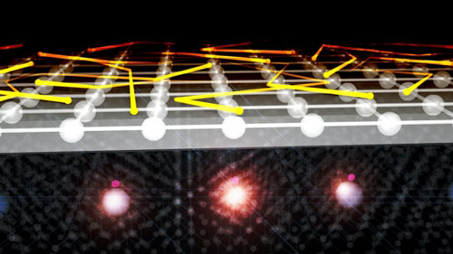 |
| Graphic depiction of NV center sensors (red glowing spheres) used to probe electron motion in a conductor. (Image: JQI)
|
|
Diamond, which is a vast array of carbon atoms, can contain a wide variety of defects. An NV center defect is formed when a nitrogen atom substitutes for a carbon atom and is adjacent to a vacancy, or missing carbon atom, in the lattice. NV centers have discrete, atom-like energy levels that can be probed using green laser light. Like atomic systems, the NV centers can be used as a qubit. In this experiment, physicists harness the sensitivity of these isolated quantum systems to characterize electron motion.
|
|
A conductive silver sample is deposited onto a diamond substrate that contains NV centers. While these defects can occur naturally, the team here purposefully creates them approximately 15 nanometers away from the silver layer. At temperatures above absolute zero, the electrons inside of the silver layer (or any conductor) bounce around and generate random currents--this is a phenomenon known as Johnson noise. Since electrons are charged particles, their motion results in fluctuating magnetic fields, which extend outside of the conductor.
|
|
Typically, changing magnetic fields can wreak all sorts of havoc, including for the nearby NV centers. Here, each NV center is used as a sensor that can be thought of as switching between two states, 1 and 0. The sensor can be calibrated in the presence of a constant magnetic field such that it is in state 1. If the sensor experiences an oscillating magnetic field, the sensor switches to state 0. There is one more important component to this sensor--it can detect magnetic field strength as well. For weak magnetic field fluctuations, the NV sensor will slowly decay to state 0; for stronger fluctuations, it will decay much faster from 1 to 0. By detecting different decay times, physicists can precisely measure the fluctuating magnetic fields, which tells them about the electron behavior at a very small length scale. Like any good sensor, the NV centers are almost completely non-invasive—their read-out with laser light does not disturb the sample they are sensing.
|
|
The team studied the scaling of the magnetic noise with different parameters such as temperature and distance from the silver surface and found excellent agreement with theoretical predictions. In addition, by changing the nature of the silver sample from “polycrystalline” to “single-crystalline” they were able to observe a dramatic difference in the behavioral trends of the magnetic field noise, particularly as the sample was cooled. In polycrystalline samples, atoms are not arranged in a regular repeating lattice over long distances, thus electrons travel don’t travel very far-- roughly 10 nanometers or less-- before scattering off an obstacle. These frequent collisions are the main source of field noise in polycrystalline materials. In contrast, a single crystal is uniform at these length scales and electrons can travel over 100 times farther. The electron movement, and corresponding magnetic field noise from the single silver crystal is a departure from so-called Ohmic predictions of the polycrystalline case, and the team was able to explore both of these extremes non-invasively.
|
|
These results demonstrate that single NV centers can be used to directly study electron behavior inside of a conductive material on the nanometer length scale. Notably, this technique does not require electrical leads, applied voltages, or even physical contact with the sample of interest, thus enabling the measurement of much smaller or more fragile samples. Future applications of this technique include the study of complex condensed matter phenomena, as well as metrology for commercial materials science.
|