| Posted: Nov 26, 2015 |
Physicists develop new technique to fathom 'smart' materials with graphene
(Nanowerk News) Physicists from the FOM Foundation and Leiden University have found a way to better understand the properties of manmade 'smart' materials. Their method reveals how stacked layers in such a material work together to bring the material to a higher level. Group leader Sense Jan van der Molen and his research team will publish their results on 26 November 2015 in Nature Communications ("Nanoscale measurements of unoccupied band dispersion in few-layer graphene").
|
|
Can we design smart materials with entirely new properties? A highly promising way of doing this is to stack extremely thin layers – just one atom thick – into a three-dimensional material; a sort of sandwich cake. Interestingly enough, the properties of these composite materials are not only determined by the properties of the individual layers. The interaction between the layers also plays a significant role. Consequently, such a layered material can have very different properties than you might expect based on the combination of properties of the individual layers; the whole is more than the sum of the parts. Physicists from FOM and Leiden University have developed a technique that allows them to study the interaction between the material layers.
|
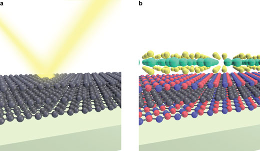 |
| Smart materials. a) The new measurement technique fires electrons at the stacked materials at an angle. By analysing the reflection of the electrons, researchers can better understand how the two dimensional layers work together to establish the properties of the combined material. b) The long term goal is for researchers to design new materials, by building a 'sandwich cake' of material layers with the exact desired properties. (Image: Johannes Jobs)
|
|
Band structure
|
|
The electronic properties of a material, expressed in what is called the band structure, determine how the material behaves. The band structure tells you what energy an electron in the material can have and how this energy depends on the velocity of the electron. There are allowed energies ('bands') and forbidden energies ('band gaps'). A large part of this band structure was previously difficult to measure. First author Johannes Jobst and his colleagues overcame the problem by using and upgrading a special microscope: a Low-Energy Electron Microscope (LEEM).
|
|
The microscope fires electrons with a specific energy at the probed material. Researchers subsequently measure how many electrons of various energies are reflected. When an incoming electron encounters an unoccupied state in the material, it is not reflected. Conversely, when there are no free states with the energy of the incoming electron, the reflection rate is high. Using this method, the researchers can measure which occupied and unoccupied electron states are present in the layered material and consequently what the band structure looks like.
|
|
By doing this with various stacks of graphene, the researchers managed to reveal how the bands associated with the different layers interact with each other. The method has a 100,000 times higher spatial resolution than conventional methods. This is important because the current layered materials have an extremely small surface (far smaller than a square millimetre).
|
|
Designer materials
|
|
As soon as scientists have a good understanding of the interaction, they might be able to take the next step: "We want to be able to choose certain properties in advance and subsequently stack the layers in such a way to realise the desired material," says Sense Jan van der Molen. "Such designer materials are the long-term objective."
|