| Posted: Aug 29, 2016 |
Electronic circuits printed at 1 micron resolution
(Nanowerk News) A research team consisting of MANA Independent Scientist Takeo Minari, International Center for Materials Nanoarchitectonics (MANA), NIMS, and Colloidal Ink developed a printing technique for forming electronic circuits and thin-film transistors (TFTs) with line width and line spacing both being 1 µm (Advanced Materials, "Spontaneous Patterning of High-Resolution Electronics via Parallel Vacuum Ultraviolet").
|
|
Using this technique, the research team formed fully-printed organic TFTs with a channel length of 1 µm on flexible substrates, and confirmed that the TFTs operate at a practical level.
|
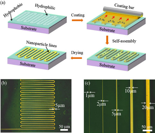 |
| Formation of microcircuit lines using a selective coating technique. (a) Schematic of selective coating technique. Only a hydrophilic region created through irradiation of parallel vacuum ultraviolet (PVUV) is coated with metal ink. (b) Electronic circuit with a line width of 5 µm formed through selective coating. (c) Electrode lines with different widths. Lines as narrow as 1 µm can be formed.
|
|
Printed electronics—printing techniques to fabricate electronic devices using functional materials dissolved in ink—is drawing much attention in recent years as a promising new method to create large-area semiconductor devices at low cost. Because these techniques enable the formation of electronic devices even on flexible substrates, they are expected to be applicable to new fields such as wearable devices. In comparison, conventional printing technologies allow the formation of circuits and devices with line widths only as narrow as several dozen micrometers. Accordingly, they are not applicable to the creation of minute devices suitable for practical use. Thus, there were high expectations for developing new printing techniques capable of consistently fabricating circuits with line widths of several micrometers or less.
|
|
In this study, the research team developed a printing technique capable of forming metal circuits with line width being 1 µm on flexible substrates. Using this technique, they fabricated minute organic TFTs. The principle of this printing technique is as follows: First, form hydrophilic and hydrophobic micro-patterns on the substrate by irradiating it with parallel vacuum ultraviolet (PVUV) at a wavelength of 200 nm or less. Then, coat only the hydrophilic patterns with metal nanoparticle inks. The use of a PVUV light source (Ushio Inc.) enabled us to focus emitted light on much smaller targets than conventional light sources.
|
|
Moreover, the use of DryCure-Au—metal nanoparticle ink that can form a conductive film at room temperature developed by Colloidal Ink—enabled us to form devices and circuits at room temperature during the entire process. As a result, we are able to fully prevent distortion of flexible substrates by heat, and form and laminate circuits within the accuracy of several microns. In addition, we precisely tuned the gate overlap lengths of the printed organic TFTs fabricated by this technique, which was previously impossible due to accuracy issues. As a result, a practical mobility level of 0.3 cm2 V-1 s-1 was accomplished for the organic TFTs with the channel length of 1 µm.
|
|
In future studies, we will aim to apply the technique in various fields such as large-area flexible displays and sensors. Since the process we developed is applicable to bio-related materials, the technique may also be useful in medical and bioelectronics fields.
|