| Posted: Nov 04, 2010 |
|
Easy fabrication of non-reflecting and self-cleaning silicon and plastic surfaces
|
|
(Nanowerk News) The Microfabrication group of Aalto University which specializes in microfabrication and microfludics has developed a new and rapid method for fabrication of non-reflecting and self-cleaning surfaces. Surface properties are based on the nanostructured surface. The research results were just published in the journal Advanced Materials ("Non-Reflecting Silicon and Polymer Surfaces by Plasma Etching and Replication").
|
|
The most laborious part the fabrication process was excluded when the Aalto University's Microfabrication group developed a novel maskless method for fabrication of pyramid-shaped nanostructures on a silicon surface using deep reactive ion etching. The nanostructured silicon wafer can be further used as a template to create an ealstomeric stamp, which can be used to replicate the original non-reflective and self-cleaning nanostructure into the different polymers.
|
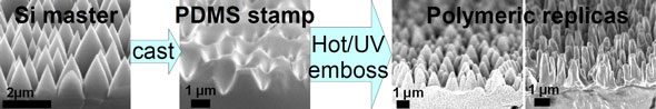 |
| Scanning electron microscopy images of the nanostructured silicon surface made by the maskless plasma etching method; the elastomeric stamp replicated from the silicon surface and the nanostructure replicated to two different polymers using the elastomeric stamp. Both the original silicon surface and the replicated polymer surfaces are non-reflecting and self-cleaning.
|
|
Smooth silicon surfaces are mirror-like and they reflect more than 50 percent of incoming light, while nanostructured silicon and polymeric surfaces are almost completely non-reflecting. The reflectance is reduced at broad wavelength range due to smooth refractive index transition from air to substrate because of the nanostructures, says Lauri Sainiemi from Microfabrication group.
|
|
Non-reflecting surfaces and their fabrication methods are hot research topics because they are needed in realization of more efficient solar cells. Similar nanostructured silicon and polymeric surfaces can also be utilized in chemical analysis, because low reflectance is needed in analysis procedure. The second beneficial property of the surfaces is self-cleaning, which is based on nanostructures, which are coated with a thin low surface energy film.
|
|
The applications of the developed nanofabrication methods for silicon and polymers range from sensors to solar cells. The biggest strength of the fabrication methods is their scalability and possibility to large scale industrial manufacturing. I believe that there is interest because our fabrication methods enable simple and low-cost manufacturing of nanostructures on large areas and the methods are compatible with single-crystalline, poly-crystalline and amorphous silicon as well as wide variety of different polymers, concludes Sainiemi.
|
|
The group has already developed surfaces for chemical analysis of drugs in collaboration with other research groups and that research will continue in future. An interesting novel field is the development of more effective self-cleaning and dirt-repellant surfaces that would especially benefit solar cell research. The fabrication of water-repellent surfaces is fairly straightforward, but liquids with low surface tension can still contaminate the surface. At the moment we are developing novel surfaces that also repel oily liquids.
|