| Aug 29, 2016 | |
New solar cell is more efficient, costs less than its counterparts |
|
| (Nanowerk News) The cost of solar power is beginning to reach price parity with cheaper fossil fuel-based electricity in many parts of the world, yet the clean energy source still accounts for slightly more than 1% of the world’s electricity mix. | |
| To boost global solar power generation, researchers must overcome some of the technological limitations that are preventing solar power from scaling up even further, which includes the inability to develop very high-efficiency solar cells – solar cells capable of converting a significant amount of sunlight into usable electrical energy – at very low costs. | |
| A team of researchers from the Masdar Institute and the Massachusetts Institute of Technology (MIT) may have found a way around the seemingly inseparable high-efficiency and high-cost linkage through an innovative multi-junction solar cell that leverages a unique “step-cell” design approach and low cost silicon. The new step-cell combines two different layers of sunlight-absorbing material to harvest a broader range of the sun’s energy while using a novel, low-cost manufacturing process. | |
| The team’s step-cell concept can reach theoretical efficiencies above 40% and estimated practical efficiencies of 35%, prompting the team’s principal investigators – Masdar Institute’s Dr. Ammar Nayfeh, Associate Professor of Electrical Engineering and Computer Science, and MIT’s Dr. Eugene Fitzgerald, the Merton C. Flemings - SMA Professor of Materials Science and Engineering – to plan a start-up company to commercialize the promising solar cell. | |
 |
|
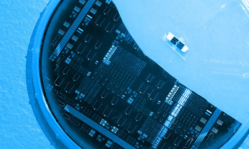
| A silicon solar cell with silicon-germanium filter using a step-cell design (large) and a gallium arsenide phosphide layer on silicon step-cell proof-of-concept solar cell (small). (Image: Tahra Al Hammadi, Masdar Institute) | |
| Dr. Fitzgerald has launched several start-ups, including AmberWave Systems Corporation, Paradigm Research LLC, and 4Power LLC. The MIT professor thinks the step-cells might be ready for the PV market within the next year or two. | |
| RATIONALE | |
| In order to increase the global share of solar power, solar photovoltaics (PV) need to move away from traditional silicon crystalline solar cells, which have been touted as the industry’s gold standard in terms of efficiency for over a decade. In fact, some estimates report that over 90% of global solar PV installations are single-junction, crystalline silicon solar cells. | |
| This is because silicon-based solar cells are relatively cheap to manufacture, but the problem is that they are not very efficient at converting sunlight into electricity. On average, solar panels made from silicon-based solar cells convert between 15% and 20% of the sun’s energy into usable electricity. | |
| Silicon’s low sunlight-to-electrical energy efficiency is partially due to its bandgap; the bandgap prevents the semiconductor from efficiently converting higher energy photons, such as those emitted by blue, green and yellow light waves, into electrical energy. Instead, only the lower energy photons, such as those emitted by the longer red light waves, are efficiently converted into electricity. | |
| To harness more of the sun’s higher energy photons, scientists have explored different semiconductor materials, such as gallium arsenide and gallium phosphide. While these semiconductors have reached higher efficiencies than silicon, the highest efficiency solar cells have been made by layering different semiconductor materials on top of each other and fine-tuning them to absorb a different slice of the electromagnetic spectrum. | |
| These layered cells, known as multi-junction solar cells, can reach theoretical efficiencies upwards of 50%, but their very high manufacturing costs are preventing them from entering the mainstream solar cell market, relegating their use to niche applications, like satellites and other specialized applications where high costs are less important than low weight and high efficiency. | |
| The Masdar Institute-MIT step-cell, which can be manufactured at a fraction of the cost of traditional multi-junction solar cells, may be the critical solution needed to boost commercial applications of high-efficiency, multi-junction solar cells at the industrial level. | |
| PROJECT BRIEF | |
| The innovative “step-cell” is made by layering gallium arsenide phosphide-based solar cells, a semiconductor material that absorbs and efficiently converts higher energy photons, on a low cost silicon solar cell, creating a tandem solar cell that could ultimately achieve a practical power efficiency of approximately 35%. | |
|
The step-cell creates a literal “step” between the top gallium arsenide phosphide layer and the bottom silicon layer. The silicon layer is exposed, appearing like a bottom step. This intentional step design allows the top gallium arsenide phosphide layer to absorb the high energy photons (from blue, green and yellow light) leaving the bottom silicon layer free to absorb not only lower energy photons (from red light) transmitted through top layers, but also the entire visible light spectrum.
The unique design ensures that the silicon cell below can receive more photons in the exposed “step” part, increasing the solar cell’s efficiency. This “step” can be used as a new design optimization parameter, with the added benefits of low-cost manufacturing process. “We realized that when the top gallium arsenide phosphide layer completely covered the bottom silicon layer, the lower energy photons were absorbed by the silicon germanium – the substrate on which the gallium arsenide phosphide is grown – and thus the solar cell had a much lower efficiency,” explained Sabina Abdul Hadi, a PhD student at Masdar Institute whose doctoral dissertation provided the foundational research for the step-cell. |
|
| “By etching away the top layer and exposing some of the silicon layer, we were able to increase the efficiency considerably,” she added. She was one of 9 PhD candidates to receive her doctoral degree at Masdar Institute’s sixth annual commencement, which was held earlier this month. | |
| Abdul Hadi, who worked under the supervision of Dr. Nayfeh, conducted simulations based on experimental results to determine the optimal levels and geometrical configuration of the gallium arsenide phosphide layer on silicon to yield the highest efficiencies. Her findings resulted in the team’s initial proof-of-concept solar cell. Abdul Hadi will continue supporting the step-cell’s technological development as a post-doctoral researcher at Masdar Institute. | |
| “I am very proud of what Sabina accomplished during her PhD studies. She is an ideal PhD student and her work covers theoretical, simulation, proof of concept fabrication, and cost analysis. We are thrilled she will transition to a post-doctoral position and help to develop and commercialize step cell technologies,” said Dr. Nayfeh. | |
| On the MIT side, the team developed the gallium arsenide phosphide, which they did by growing the semiconductor alloy on a substrate made of silicon germanium. | |
| “Gallium arsenide phosphide cannot be grown directly on silicon, because its crystal lattices differ considerably from silicon’s, so the silicon crystals become degraded. That’s why we grew the gallium arsenide phosphide on the silicon germanium – it provides a more stable base,” explained Dr. Nayfeh. | |
| The problem with the silicon germanium under the gallium arsenide phosphide layer is that silicon germanium absorbs the lower energy light waves before it reaches the bottom silicon layer, and silicon germanium does not convert these low energy light waves into current as it is not an active part of the cells in that multi-junction setup. | |
| “To get around the optical problem posed by the silicon germanium, we developed the idea of the step-cell, which allows us to leverage the different energy absorption bands of gallium arsenide phosphate and silicon,” said Dr. Nayfeh. | |
| Explaining the future low-cost fabrication process, Dr. Fitzgerald said: “We grew the gallium arsenide phosphide on top of the silicon germanium, patterned it in the optimized geometric configuration, and bonded it to a silicon cell. Then we etched through the patterned channels and lifted off the silicon germanium alloys on silicon. What remains then, is a high-efficient tandem solar cell and a silicon germanium template, ready to be re-used.” | |
| Because the tandem cell is bonded together, rather than created as a monolithic solar cell (where all layers are grown onto a single substrate), the silicon germanium can be removed and re-used repeatedly, which significantly reduces the manufacturing costs. | |
| “Adding that one layer of the gallium arsenide phosphide can really boost efficiency of the solar cell but because of the unique ability to etch away the silicon germanium and re-use it, the cost is kept low because you can amortize that silicon germanium cost over the course of manufacturing many cells,” he added. | |
| The team’s research findings are reported at the 40th and 42nd annual IEEE PVSC conference with the work being awarded Best Poster at the 42nd IEEE PVSC conference. In addition, the initial “step-cell” proof of concept cell will be presented June 8th 2016 at the 43rd IEEE PVSC in Portland Oregon. Also, more detailed journal papers are published on the team’s research in the Journal of Applied Physics ("Theoretical efficiency limit for a two-terminal multi-junction “step-cell” using detailed balance method") and IEEE Journal of Photovoltaics ("Design Optimization of Single-Layer Antireflective Coating for GaAs1-xPx/Si Tandem Cells With x=0, 0.17, 0.29, and 0.37"). | |
| APPLICATIONS/IMPACT | |
| Dr. Fitzgerald believes the step-cell fits perfectly in the existing gap of the solar PV market, between super high-efficiency (which is dominated by expensive PV systems used in satellites and other niche applications) and the low-efficiency industrial market. This positions it uniquely in the marketplace, and as volume increases in this market gap, the manufacturing costs will be driven down even further over time. | |
| This project began as one of nine Masdar Institute-MIT Flagship Research Projects, which are high-potential projects involving faculty and students from both universities. | |
| “This research project highlights the valuable role that research and international collaboration plays in developing a commercially-relevant technology-based innovation, and it is a perfect demonstration of how a research idea can transform into an entrepreneurial reality,” said Dr. Nayfeh. | |
| The novel, silicon based multi-junction “step” solar cell developed through this collaborative research project directly contributes to the development of highly-skilled human capital and innovative technological systems needed to fuel the UAE’s knowledge-economy transformation. |
| Source: By Erica Solomon, Masdar Institute |