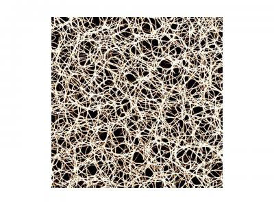
 The development of a new measurement technology under a research project funded by the Air Force Office of Scientific Research and the National Science Foundation is probing the structure of composite and biological materials.
Mar 11th, 2011
Read more
Everything moves! But in a world dominated by electronic devices it is easy to forget that all measurements involve motion, whether it is motion of electrons through a transistor, or the simple displacement of a mechanical element. New EU-funded research suggests that quantum mechanics may hold the answer to when motion will die out.
Mar 11th, 2011
Read more
UCLA nanotechnology research mimics enzymes in directing chemical reactions.
Mar 10th, 2011
Read more
The Society of Manufacturing Engineers unveils its annual innovations list.
Mar 10th, 2011
Read more
University of Illinois engineers have developed a form of ultra-low-power digital memory that is faster and uses 100 times less energy than similar available memory. The technology could give future portable devices much longer battery life between charges.
Mar 10th, 2011
Read more
Northwestern University researchers have developed a new switching device that takes quantum communication to a new level. The device is a practical step toward creating a network that takes advantage of the mysterious and powerful world of quantum mechanics.
Mar 10th, 2011
Read more
When prostate cancer stem cells were enclosed in self-assembling nanomaterials made of peptides (SAP), the SAP stopped cancer stem cell colony formation and also stopped the division of cancer cells in laboratory cultures (in vitro). According to the international team of researchers who built and tested the nano-sized traps, the cancer cells grew and multiplied after they were "liberated" from their SAP prisons.
Mar 10th, 2011
Read more
According to the Project on Emerging Nanotechnologies (PEN) over 1,300 manufacturer-identified, nanotechnology-enabled products have entered the commercial marketplace around the world.
Mar 10th, 2011
Read more
Researchers are developing computational models to predict the behaviour of nanomaterials in biological systems. Such predictions will allow researchers to streamline and prioritise the toxicological testing of nanomaterials.
Mar 10th, 2011
Read more
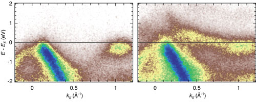 How fast an intense laser pulse can change the electrical properties of solids is revealed by researchers from Kiel University.
Mar 10th, 2011
Read more
The regions of the world see printed electronics differently. For example, the USA focuses on the military applications among others. East Asia wishes to use printed electronics to reinforce its dominance in electronic displays. Europe has interest in a very wide range of potential applications, with consumer packaged goods being just one of many applicational sectors prioritised.
Mar 10th, 2011
Read more
 Lasers used to study splicing of pre-messenger RNA molecules.
Mar 10th, 2011
Read more
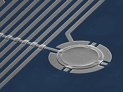 Physicists have demonstrated an electromechanical circuit in which microwaves communicate with a vibrating mechanical component 1,000 times more vigorously than ever achieved before in similar experiments. This apparatus is a new tool for processing information and potentially could control the motion of a relatively large object at the smallest possible, or quantum, scale.
Mar 9th, 2011
Read more
Nanodiamond-drug combo significantly improves treatment of chemotherapy-resistant cancers.
Mar 9th, 2011
Read more
 Springy nanostructured metals hold promise of making engines, medical equipment, security systems more efficient and effective.
Mar 9th, 2011
Read more
Tomorrow's nonvolatile memory devices - computer memory that can retain stored information even when not powered - will profoundly change electronics, and Cornell University researchers have discovered a new way of measuring and optimizing their performance.
Mar 9th, 2011
Read more
 Subscribe to our Nanotechnology News feed