Focused Ion Beam Milling: Precision Nanofabrication at the Nanoscale
What is Focused Ion Beam Milling?
Focused ion beam (FIB) milling is a nanofabrication technique that uses a focused beam of ions to precisely mill, etch, or deposit materials at the nanoscale. It enables the creation of high-resolution nanostructures, cross-sectional analysis, and site-specific material modification. FIB milling has become an essential tool in various fields, including materials science, semiconductor industry, and biological research.
Principles of Focused Ion Beam Milling
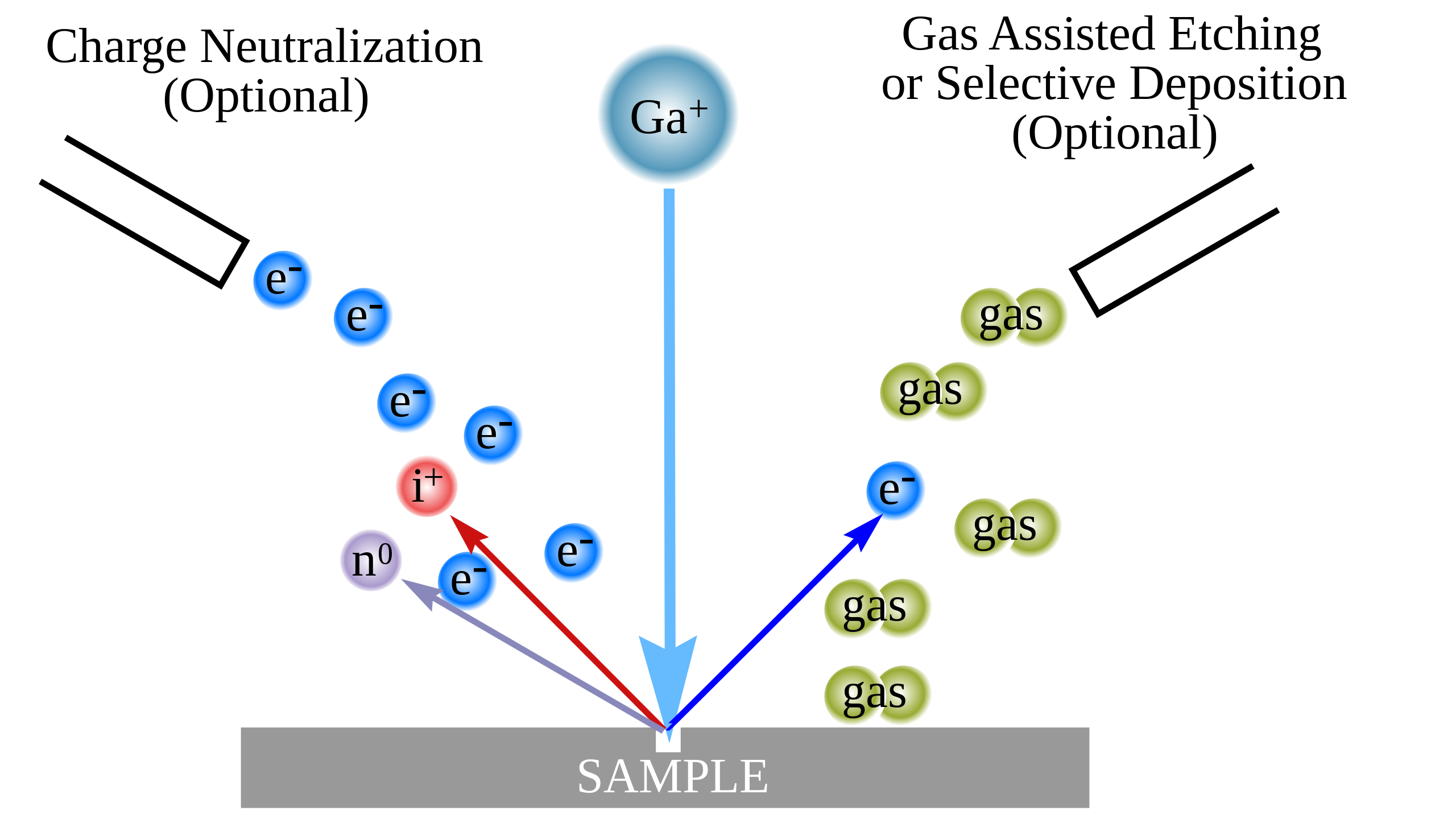
FIB milling relies on the interaction between a focused beam of ions and the sample surface. The most commonly used ion source is liquid metal ion source (LMIS), typically gallium (Ga+), due to its low melting point and high stability. The ions are extracted from the source, accelerated, and focused onto the sample surface using electrostatic lenses.
When the high-energy ions strike the sample surface, they interact with the material through various mechanisms, including sputtering, ion implantation, and secondary electron emission. By controlling the ion beam parameters, such as beam current, accelerating voltage, and dwell time, precise milling or etching of the sample can be achieved at the nanoscale.
Capabilities of Focused Ion Beam Milling
FIB milling offers several unique capabilities for nanofabrication:
- High Resolution: FIB milling can achieve feature sizes down to a few nanometers, enabling the fabrication of intricate nanostructures and devices. The resolution is determined by factors such as ion beam size, ion-sample interaction volume, and the material's properties.
- Site-Specific Milling: FIB milling allows for precise, site-specific material removal or modification. By controlling the ion beam position and dwell time, specific regions of the sample can be selectively milled or etched, enabling the creation of complex nanostructures and the preparation of samples for cross-sectional analysis.
- Material Deposition: In addition to milling, FIB systems can also be used for material deposition. By introducing gaseous precursors into the chamber, the ion beam can induce localized chemical vapor deposition (CVD), allowing for the precise deposition of metals, oxides, or other materials at specific sites on the sample.
- Imaging and Analysis: FIB systems are often equipped with secondary electron detectors, enabling high-resolution imaging of the sample surface. This imaging capability allows for real-time monitoring of the milling process and facilitates the alignment and positioning of the ion beam. Additionally, FIB can be combined with other analytical techniques, such as energy-dispersive X-ray spectroscopy (EDS) or electron backscatter diffraction (EBSD), for compositional and crystallographic analysis of the milled structures.
Applications of Focused Ion Beam Milling
FIB milling finds applications in various fields, leveraging its high-resolution and site-specific nanofabrication capabilities:
Materials Science
FIB milling is extensively used in materials science for the preparation of samples for transmission electron microscopy (TEM) analysis. By milling thin lamellae or cross-sections of materials, FIB enables the study of microstructure, defects, and interfaces at the nanoscale. FIB is also used for the fabrication of micro- and nano-electromechanical systems (MEMS/NEMS) devices, such as sensors, actuators, and resonators.
Semiconductor Industry
In the semiconductor industry, FIB milling plays a crucial role in the failure analysis and debugging of integrated circuits. By selectively milling and exposing specific regions of the chip, FIB enables the identification and characterization of defects, shorts, and other manufacturing issues. FIB is also used for circuit editing, allowing for the modification or repair of integrated circuits at the nanoscale.
Biological Research
FIB milling has found applications in biological research, particularly in the preparation of samples for electron microscopy. By milling thin sections of biological tissues or cells, FIB enables the study of ultrastructural features and the localization of specific molecules. FIB can also be used for the fabrication of microfluidic devices and lab-on-a-chip systems for biological analysis and drug discovery.
Comparative Analysis
FIB milling offers unique capabilities compared to other nanofabrication techniques. Here, we compare FIB milling with electron beam lithography (EBL) and atomic force microscopy (AFM) based nanofabrication:
FIB Milling vs. Electron Beam Lithography
EBL is another high-resolution nanofabrication technique that uses a focused electron beam to pattern resist materials. While both FIB milling and EBL can achieve nanoscale resolution, they have distinct differences:
- Direct vs. Indirect Patterning: FIB milling directly removes or modifies the material, whereas EBL patterns a resist layer that requires subsequent etching or deposition steps to transfer the pattern to the substrate.
- Materials Compatibility: FIB milling can be used on a wide range of materials, including metals, semiconductors, and insulators. EBL is primarily used with electron-sensitive resists and may have limitations with certain materials.
- Speed and Throughput: EBL typically has higher throughput than FIB milling, as it can pattern larger areas in a single exposure. FIB milling is more suitable for site-specific modifications and smaller-scale patterning.
FIB Milling vs. AFM-Based Nanofabrication
AFM-based nanofabrication techniques, such as dip-pen nanolithography (DPN) and nanoscale scratching, use an AFM tip to directly manipulate materials at the nanoscale. Compared to FIB milling:
- Resolution: AFM-based techniques can achieve higher resolution than FIB milling, with the ability to manipulate materials at the atomic or molecular level. FIB milling is limited by the ion beam size and ion-sample interaction volume.
- Material Removal vs. Addition: FIB milling primarily focuses on material removal through sputtering, while AFM-based techniques can both remove and add materials through mechanical or chemical interactions between the tip and the sample.
- Throughput: FIB milling generally has higher throughput compared to AFM-based techniques, which are limited by the serial nature of the process and the speed of the AFM tip movement.
The choice between FIB milling and other nanofabrication techniques depends on the specific application requirements, such as resolution, materials compatibility, throughput, and the desired type of material modification. In some cases, a combination of techniques may be used to leverage the strengths of each method for optimal results.
Challenges and Future Perspectives
While FIB milling offers unique capabilities for nanofabrication, it also presents some challenges. One of the main challenges is the potential damage to the sample caused by the high-energy ion beam. Ion implantation, amorphization, and gallium contamination can occur during the milling process, which may alter the properties of the material. Careful optimization of the milling parameters and the use of protective layers can mitigate these effects.
Future advancements in FIB milling will focus on improving the resolution, throughput, and versatility of the technique. The development of new ion sources, such as helium and neon ions, can provide higher resolution and reduced sample damage compared to traditional gallium ions. The integration of FIB with other nanofabrication techniques, such as electron beam lithography and atomic layer deposition, will enable the creation of multifunctional nanostructures and devices. Additionally, the automation of FIB milling processes and the development of user-friendly software will facilitate the widespread adoption of FIB in various research and industrial settings.
Further Reading
Journal of Micromechanics and Microengineering, A review of focused ion beam applications in microsystem technology
