Nanopatterning: Crafting Nanostructures with Precision
What is Nanopatterning?
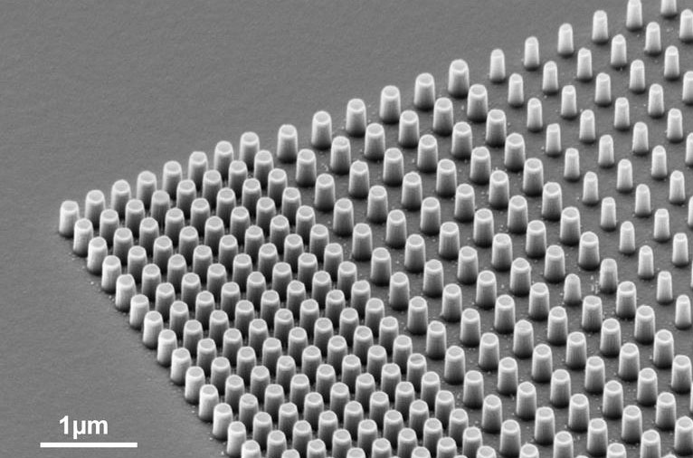
Nanopatterning is the process of creating ordered structures or patterns at the nanoscale, typically with dimensions below 100 nanometers. It involves the precise manipulation and control of materials to fabricate nanoscale features, such as grooves, dots, lines, or more complex geometries. Nanopatterning plays a crucial role in various fields, including nanoelectronics, photonics, biosensors, and data storage, enabling the development of advanced devices and systems.
Nanopatterning Techniques
Several nanopatterning techniques have been developed to create nanoscale patterns with high resolution and precision:
Lithography-Based Techniques
- Photolithography: Photolithography uses light to transfer a geometric pattern from a photomask to a light-sensitive chemical (photoresist) on a substrate. It is widely used in the semiconductor industry for fabricating integrated circuits.
- Electron Beam Lithography (EBL): Electron Beam Lithography uses a focused electron beam to directly write patterns on an electron-sensitive resist. It offers higher resolution than photolithography but is slower and more expensive.
- Nanoimprint Lithography (NIL): Nanoimprint Lithography involves pressing a mold with nanoscale features onto a resist-coated substrate, followed by the removal of the mold. It enables high-throughput and low-cost nanopatterning.
Self-Assembly Techniques
- Block Copolymer Lithography: Block copolymers are composed of two or more chemically distinct polymer segments that can self-assemble into periodic nanostructures. By controlling the block copolymer composition and processing conditions, various nanoscale patterns can be obtained.
- Colloidal Lithography: Colloidal lithography uses self-assembled arrays of colloidal particles as masks for patterning underlying substrates. It enables the fabrication of large-area nanostructures with tunable sizes and shapes.
Direct Writing Techniques
- Dip-Pen Nanolithography (DPN): Dip-Pen Nanolithography uses an atomic force microscope (AFM) tip to directly write patterns on a substrate by depositing molecules or materials. It allows for the precise positioning and patterning of functional materials at the nanoscale.
- Focused Ion Beam (FIB) Milling: FIB milling uses a focused beam of ions to directly remove or deposit materials on a substrate, enabling the fabrication of complex 3D nanostructures.
Applications of Nanopatterning
Nanopatterning has enabled the development of various advanced applications:
Nanoelectronics
Nanopatterning is essential for fabricating high-density and high-performance nanoelectronic devices, such as transistors, memory devices, and sensors. By creating nanoscale features, researchers can achieve enhanced device performance, reduced power consumption, and increased integration density.
Photonics and Optoelectronics
Nanopatterning techniques are used to create photonic crystals, plasmonic structures, and metamaterials with unique optical properties. These nanostructures find applications in light-emitting diodes (LEDs), solar cells, optical sensors, and integrated photonic circuits.
Biosensors and Biomedical Devices
Nanopatterning plays a crucial role in the development of biosensors and biomedical devices. By creating nanoscale patterns on sensor surfaces, researchers can enhance the sensitivity, selectivity, and limit of detection for various analytes, such as proteins, nucleic acids, and cells. Nanopatterned surfaces also find applications in tissue engineering, drug delivery, and implantable devices.
Data Storage
Nanopatterning enables the fabrication of high-density data storage devices, such as magnetic and optical storage media. By creating nanoscale patterns on the storage media, researchers can achieve higher storage capacities and faster data access rates.
Challenges and Future Perspectives
Despite the significant advancements in nanopatterning techniques, several challenges need to be addressed. One of the main challenges is the scalability and throughput of nanopatterning processes, particularly for large-area and high-volume manufacturing. Additionally, the integration of different nanopatterning techniques and materials to create complex, multi-functional nanostructures remains a challenge.
Future research in nanopatterning will focus on the development of novel patterning techniques with improved resolution, throughput, and cost-effectiveness. The integration of nanopatterning with other technologies, such as 3D printing, self-assembly, and bio-inspired approaches, will enable the fabrication of advanced nanostructures with unprecedented properties and functionalities. Furthermore, the exploration of nanopatterning for emerging applications, such as quantum computing, neuromorphic engineering, and personalized medicine, will drive the field forward.
