Piezoresponse Force Microscopy (PFM): Nanoscale Imaging of Electromechanical Properties
Definition: Piezoresponse Force Microscopy (PFM) is a scanning probe microscopy technique that enables nanoscale imaging and characterization of electromechanical properties in piezoelectric and ferroelectric materials. PFM measures the local electromechanical response of a sample to an applied electric field, providing insights into domain structures, polarization dynamics, and local piezoelectric coefficients.
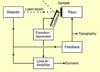
Electronic circuit for PFM operation. (Image: Dr. Elisabeth Soergel, University of Bonn)
Principle of Operation
PFM is based on the converse piezoelectric effect, where an applied electric field induces mechanical strain in piezoelectric materials. In PFM, an AC voltage is applied between a conductive atomic force microscope (AFM) tip and the sample, generating a local electric field. This electric field causes the sample to expand or contract locally due to the converse piezoelectric effect. The resulting surface deformation is detected by the AFM tip as a vertical deflection, which is proportional to the local piezoelectric coefficient and polarization orientation.
By scanning the AFM tip across the sample surface and measuring the tip deflection at each point, PFM generates high-resolution maps of the piezoresponse amplitude and phase. The piezoresponse amplitude provides information about the magnitude of the local electromechanical response, while the phase reveals the polarization orientation (domain structure) of the sample.
Modes of Operation
PFM can be operated in different modes to obtain complementary information about the sample's electromechanical properties:
- Vertical PFM (VPFM): VPFM measures the out-of-plane piezoresponse, i.e., the surface deformation perpendicular to the sample surface. It is sensitive to the vertical component of the polarization vector and is commonly used to study domain structures and polarization switching dynamics in thin films and nanostructures.
- Lateral PFM (LPFM): LPFM detects the in-plane component of the piezoresponse, i.e., the surface deformation parallel to the sample surface. It provides information about the lateral polarization component and is particularly useful for studying domain walls and in-plane polarization switching.
- Resonance-Enhanced PFM: This mode exploits the contact resonance of the AFM cantilever to amplify the piezoresponse signal. By operating at or near the contact resonance frequency, the sensitivity and signal-to-noise ratio of PFM measurements can be significantly improved.
Applications
PFM has found widespread applications in the fields of materials science, nanotechnology, and condensed matter physics. Some key applications include:
- Ferroelectric Domain Imaging: PFM is widely used to visualize and characterize ferroelectric domain structures at the nanoscale. It enables the mapping of domain polarization, domain walls, and polarization switching dynamics, providing insights into the fundamental properties and behavior of ferroelectric materials.
- Piezoelectric Characterization: PFM allows the quantitative measurement of local piezoelectric coefficients, enabling the investigation of piezoelectric properties in thin films, nanostructures, and composite materials. This information is crucial for the development of piezoelectric devices such as sensors, actuators, and energy harvesters.
- Ferroelectric Memory and Data Storage: PFM plays a vital role in the development of ferroelectric random-access memory (FeRAM) and high-density data storage devices. By enabling the nanoscale manipulation and characterization of ferroelectric domains, PFM contributes to the advancement of these technologies.
- Electromechanical Coupling in Nanostructures: PFM is employed to study the electromechanical coupling and piezoelectric properties of individual nanostructures such as nanowires, nanotubes, and nanorods. Understanding the electromechanical behavior at the nanoscale is essential for the development of novel piezoelectric and electromechanical devices.
Advantages and Limitations
PFM offers several advantages over other techniques for studying electromechanical properties at the nanoscale:
- High spatial resolution, enabling nanoscale imaging of domain structures and local piezoelectric properties
- Quantitative measurement of local piezoelectric coefficients
- Non-destructive and non-invasive characterization
- Capability to study both out-of-plane and in-plane piezoresponse
However, PFM also has some limitations:
- Requires conductive samples or the use of conductive coatings
- Interpretation of PFM data can be challenging due to the complex tip-sample interactions and potential artifacts
- Limited to the study of piezoelectric and ferroelectric materials
Despite these limitations, PFM remains a powerful and widely used technique for investigating electromechanical properties at the nanoscale, contributing significantly to the advancement of materials science and nanotechnology.
To sum it up, Piezoresponse Force Microscopy (PFM) is a versatile and highly sensitive scanning probe microscopy technique that enables the nanoscale imaging and characterization of electromechanical properties in piezoelectric and ferroelectric materials. By measuring the local piezoresponse of a sample to an applied electric field, PFM provides valuable insights into domain structures, polarization dynamics, and local piezoelectric coefficients. With its high spatial resolution and quantitative capabilities, PFM has become an indispensable tool in the fields of materials science, nanotechnology, and condensed matter physics, contributing to the development of advanced piezoelectric devices and the understanding of fundamental electromechanical phenomena at the nanoscale.
Further Reading
Nature Communications, Piezoresponse force microscopy and nanoferroic phenomena
Journal of the American Ceramic Society, Electromechanical imaging and spectroscopy of ferroelectric and piezoelectric materials: State of the art and prospects for the future
