| Posted: Sep 18, 2017 |
2-D Electronics' metal or semiconductor? Both
(Nanowerk News) Modern life will be almost unthinkable without transistors. They are the ubiquitous building blocks of all electronic devices: each computer chip contains billions of them. However, as the chips become smaller and smaller, the current 3D field-electronic transistors (FETs) are reaching their efficiency limit.
|
|
A research team at the Center for Artificial Low Dimensional Electronic Systems, within the Institute for Basic Science (IBS), has developed the first 2D electronic circuit (FET) made of a single material. |
|
Published in Nature Nanotechnology, this study shows a new method to make metal and semiconductor from the same material in order to manifacture 2D FETs.
|
 |
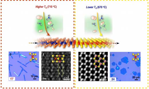
| Metallic (right) and semiconducting (left) MoTe2 crystals are obtained side by side on the same plane. Rectangular crystals represent metal MoTe2, while hexagonal crystals are the characteristic feature of semiconducting MoTe2. (click on image to enlarge)
|
|
In simple terms, FETs can be thought as high-speed switches, comprised of two metal electrodes and a semiconducting channel in between. Electrons (or holes) move from the source electrode to the drain electrode, flowing through the channel. While 3D FETs have been scaled down to nanoscale dimensions successfully, their physical limitations are starting to emerge. Short semiconductor channel lengths lead to a decrease in performance: some electrons (or holes) are able to flow between the electrodes even when they should not, causing heat and efficiency reduction.
|
|
To overcome this performance degradation, transistor channels have to be made with nanometer-scale thin materials. However, even thin 3D materials are not good enough, as unpaired electrons, part of the so-called "dangling bonds" at the surface interfere with the flowing electrons, leading to scattering.
|
 |
| The standard 3-D FET has two electrodes (source and drain, S and D) made of doped silicon and a semiconducting channel in between. When the transistor is on, the electrons move from the source to the drain passing through the channel. The 2-D FET featured in this study uses MoTe2 for both metal (red) and semiconductor (yellow), reducing off-current effects and dangling bonds which are becoming a problem with the smaller 3-D transistors. (Image: IBS)
|
|
Passing from thin 3D FETs to 2D FETs can overcome these problems and bring in new attractive properties. "FETs made from 2D semiconductors are free from short-channel effects because all electrons are confined in naturally atomically thin channels, free of dangling bonds at the surface," explains Ji Ho Sung, first author of the study. Moreover, single- and few-layer form of layered 2D materials have a wide range of electrical and tunable optical properties, atomic-scale thickness, mechanical flexibility and large bandgaps (1~2 eV).
|
|
The major issue for 2D FET transistors is the existence of a large contact resistance at the interface between the 2D semiconductor and any bulk metal. To address this, the team devised a new technique to produce 2D transistors with semiconductor and metal made of the same chemical compound, molybdenum telluride (MoTe2). It is a polymorphic material, meaning that it can be used both as metal and as semiconductor. Contact resistance at the interface between the semiconductor and metallic MoTe2 is shown to be very low. Barrier height was lowered by a factor of 7, from 150meV to 22meV.
|
|
IBS scientists used the chemical vapor deposition (CVD) technique to build high quality metallic or semiconducting MoTe2 crystals. The polymorphism is controlled by the temperature inside a hot-walled quartz-tube furnace filled with NaCl vapor: 710°C to obtain metal and 670°C for a semiconductor.
|
 |
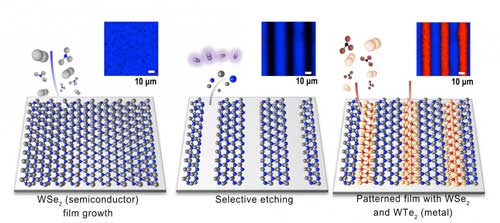
| Tungsten Diselenide (WSe2) Alternated with Tungsten Ditelluride (WTe2) can be Integrated to Form 2-D. (Image: IBS) (click on image to enlarge)
|
|
The scientists also manufactured larger scale structures using stripes of tungsten diselenide (WSe2) alternated with tungsten ditelluride (WTe2). They first created a thin layer of semiconducting WSe2 with chemical vapor deposition, then scraped out some stripes and grew metallic WTe2 on its place.
|
|
It is anticipated that in the future, it would be possible to realize an even smaller contact resistance, reaching the theoretical quantum limit, which is regarded as a major issue in the study of 2D materials, including graphene and other transition metal dichalcogenide materials.
|

