| Jul 11, 2019 |
Trapped light particles: Physicists use nanostructures to free photons for highly efficient white OLEDs(Nanowerk News) Thanks to intensive research in the past three decades, organic light-emitting diodes (OLEDs) have been steadily conquering the electronics market - from OLED mobile phone displays to roll-out television screens, the list of applications is long. |
| Current OLED research focuses in particular on improving the performance of white OLEDs for lighting elements such as ceiling or car interior lighting. These components are subject to much stricter requirements in terms of stability, angular emission and power efficiency. |
| Since light-emitting diodes only produce monochrome light, manufacturers use various additive colour-mixing processes to produce white light. |
| Since the first development of white OLEDs in the 1990s, numerous efforts have been made to achieve a balanced white spectrum and high luminous efficacy at a practical luminance level. However, the external quantum efficiency (EQE) for white OLEDs without additional outcoupling techniques can only reach 20 to 40 percent today. About 20 percent of the generated light particles (photons) remain trapped in the glass layer of the device. The reason for this is the total internal reflection of the particles at the interface between glass and air. Further photons are waveguided in the organic layers, while others get ultimately lost at the interface to the top metal electrode. |
| Numerous approaches have been investigated to extract the trapped photons from OLEDs. An international research team led by Dr. Simone Lenk and Prof. Sebastian Reineke from the TU Dresden has now presented a new method for freeing the light particles in the journal Nature Communications ("Tailor-made nanostructures bridging chaos and order for highly efficient white organic light-emitting diodes"). |
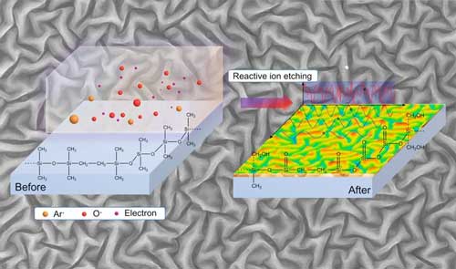 |
| Principle of reactive ion etching for the generation of quasi-periodic nanostructures. (Image: Sebastian Reineke et al., Nature Communications: CC BY 4.0) |
| The physicists introduce a facile, scalable and especially lithography-free method for the generation of controllable nanostructures with directional randomness and dimensional order, significantly boosting the efficiency of white OLEDs. The nanostructures are produced by reactive ion etching. This has the advantage that the topography of the nanostructures can be specifically controlled by adjusting the process parameters. |
| In order to understand the results obtained, the scientists have developed an optical model that can be used to explain the increased efficiency of OLEDs. By integrating these nanostructures into white OLEDs, an external quantum efficiency of up to 76.3% can be achieved. |
| For Dr. Simone Lenk, the new method opens up numerous new avenues: "We had been looking for a way to specifically manipulate nanostructures for a long time already. With reactive ion etching, we have found a cost-effective process that can be used for large surfaces and is also suitable for industrial use. The advantage lies in the fact that the periodicity and height of the nanostructures can be completely adjusted via the process parameters and that thus an optimal outcoupling structure for white OLEDs could be found. These quasi-periodic nanostructures are not only suitable as outcoupling structures for OLEDs, but also have the potential for further applications in optics, biology and mechanics". |
| Source: Technische Universität Dresden |
|
Subscribe to a free copy of one of our daily Nanowerk Newsletter Email Digests with a compilation of all of the day's news. |

