| Sep 20, 2019 |
Clarification of a new synthesis mechanism of semiconductor atomic sheet(Nanowerk News) Researchers at Tohoku University in Japan succeeded in clarifying a new synthesis mechanism regarding transition metal dichalcogenides (TMD), which are semiconductor atomic sheets having thickness in atomic order (Scientific Reports, "Nucleation dynamics of single crystal WS2 from droplet precursors uncovered by in-situ monitoring"). |
| Because it is difficult to directly observe the aspect of the growing process of TMD in a special environment, the initial growth process remained unclear, and it has been desirable to elucidate a detailed mechanism of synthesis to obtain high-quality TMD. |
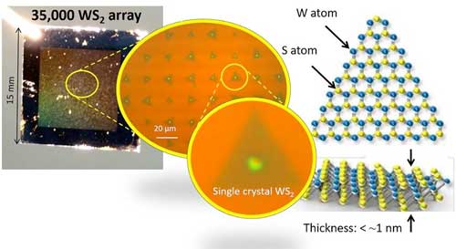 |
| Figure 1: A substrate (left photograph) that is fabricated by integrating about 35,000 monolayer single crystals of WS2, and a structural schematic of the monolayer single crystal of WS2 (right figure). (Image: Toshiaki Kato) |
| In Japan Science and Technology Agency’s Strategic Basic Research Programs, Associate Professor Toshiaki Kato and Professor Toshiro Kaneko of the Department of Electronic Engineering, Graduate School of Engineering, Tohoku University succeeded in clarifying a new synthesis mechanism regarding transition metal dichalcogenides (TMD)1), which are semiconductor atomic sheets having thickness in atomic order. |
| Because it is difficult to directly observe the aspect of the growing process of TMD in a special environment, the initial growth process remained unclear, and it has been desirable to elucidate a detailed mechanism of synthesis to obtain high-quality TMD. |
| An in-situ monitoring synthesis method2) has been developed by our research group to examine the growth aspect of TMD as a real-time optical image in a special high temperature atmosphere of about 800 °C in the presence of corrosive gases. |
| In addition, a synthesis substrate, which is a mechanism to control diffusion during the crystal growth of a precursor3), has been developed in advance; further, it has been clarified that the growing precursor diffuses a distance about 100 times larger than in conventional semiconductor materials. |
| It was also demonstrated that nucleation occurs due to the involvement of the precursor in a droplet state. Furthermore, by utilizing this method, a large-scale integration of more than 35,000 monolayer single crystal atomic sheets has been achieved on a substrate in a practical scale (Figure 1). |
| Utilizing the results of the present research, the large-scale integration of atomic-order thick4) semiconductor atomic sheets can be fabricated and is expected to be put into practical use in the field of next-generation flexible electronics. |
Notes |
| 1) Transition Metal Dichalcogenides: TMD: Atomic layer materials are similar to graphene. This material has a structure in which a transition metal is sandwiched between the chalcogen atoms. Graphene shows metallic conduction characteristics but TMD has a band gap to show semiconductor properties and is expected to be applied in the field of semiconductor devices. |
| 2) In-situ monitoring synthesis method: A crystal growing technique capable of monitoring the synthesis states in real time. |
| 3) Precursor: Raw material for crystal growing. When incorporated into the crystal, a part or all of it becomes an element constituting the crystal. |
| 4) Atomic order: The size of one atom is about several angstroms (one angstrom is one ten billionth of a meter). This means the size of one to several integrated atoms. |
| Source: Japan Science and Technology Agency |
|
Subscribe to a free copy of one of our daily Nanowerk Newsletter Email Digests with a compilation of all of the day's news. |

