| Sep 24, 2019 |
Conductive AFM (C-AFM) measurements on a polished IC surface with multiple transistor contacts |
| (Application Note) Here is a new Application Note from Nanosurf on conductive AFM (C-AFM) measurements on a polished IC surface with multiple transistor contacts. |
| Chemical-mechanical polishing (CMP) is a standard manufacturing process employed in the semiconductor industry during the fabrication of integrated circuits and memory disks. |
| When the goal is to remove surface materials, the process is referred to as chemical-mechanical polishing. |
| When the goal is to flatten the surface, it is usually referred to as chemical-mechanical planarization. The topography and electrical properties of polished surfaces can easily be characterized via AFM. |
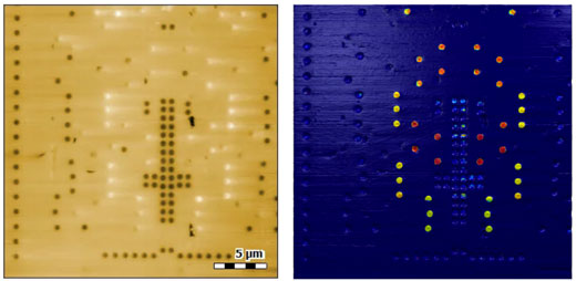 |
| Left: Topography image showing an integrated circuit structure with multiple transistor contacts (image height range: 25 nm). After polishing, contacts may appear as high or low structures on the surface. Some contacts are almost at the same height level as the surface and are thus difficult to identify in topography alone. Contacts protruding from the surface exhibit a slight "tail" towards the right. This "tail", visible in both trace and retrace, is a result of the polishing direction applied. Right: Several of the transistor contacts show a clear electric conductivity in the C-AFM image in contact mode, but at varying levels (yellow-red). Others, particularly in the central structure, some only show very low conductivity (light blue), while most contacts on the outside of the image show no conductivity at all (dark blue). Contacts with similar conductivity are clustered together ins groups and show an overall symmetrical (mirrored) arrangement. (Image: Nanosurf) |
Sample current mapped to topography |
| A current profile of the polished IC sample was generated by following a path accross the sample (and over a series of transistor contacts), as indicated in the left image below. The resulting current profile is shown on the right. |
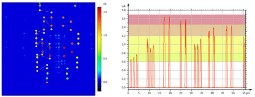 |
| (Left) Current map indicating the path of the profile as followed across the sample. The profile started at the bottom of the image crossing all high conductivity areas to the top of the image. (Right) The resulting current profile. Different levels of conductivity could be identified within the sample. (Image: Nanosurf) |
DC bias-dependent conductivity of contacts |
| Sequential imaging of the sample area with varying tip bias. On this IC sample, surface conductivity can only be observed when a negative DC bias voltage is applied to the conductive tip: |
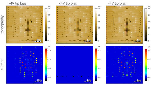 |
| At negative tip bias, certain contacts show conductive properties (Left). At positive tip bias, previously conductive contacts do not conduct (Center). Applying a negative tip bias once more restores conductivity of those contacts (Right). (Image: Nanosurf) |
Voltage I-V curves on selected locationsDepending on the location on the sample surface, voltage I-V curves show significantly different profiles. Each I-V curves was recorded on a contact and not on the base chip material. |
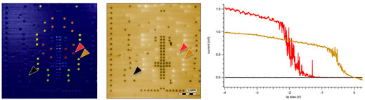 |
| Current image (Left), topography image (Center), and I-V curves (Right). Colored arrow heads indicate the locations where the I-V curves were recorded. (Image: Nanosurf) |
| Source: Nanosurf |
Subscribe to a free copy of one of our daily
Nanowerk Newsletter Email Digests
with a compilation of all of the day's news.
Nanowerk Newsletter Email Digests
with a compilation of all of the day's news.

