| Dec 09, 2019 |
Nanowire captures Abrikosov vortices(Nanowerk News) Researchers from the Moscow Institute of Physics and Technology, Lomonosov Moscow State University, and the Institute of Solid State Physics of the Russian Academy of Sciences have demonstrated the possibility of detecting the penetration of Abrikosov vortices through the superconductor/ferromagnet interface. The device is a ferromagnetic nanowire bonded to superconductive electrodes. |
| The paper was published in Scientific Reports ("Anomalous magneto-resistance of Ni-nanowire/Nb hybrid system"). |
| Superconductors are materials that lose their electrical resistance below a characteristic critical temperature ?c. Another curious property of superconductors is their ability to expel the interior magnetic field (levitation). This happens when surface currents develop, shielding the material from the magnetic field. |
| There are other superconductors, called type II. Below their critical temperatures, type II superconductors allow an external magnetic flux to penetrate the material in the form of quantized flux (vortices). This phenomenon was first predicted by Alexey Abrikosov and thus named after him. An Abrikosov vortex is a vortex of superconducting current with a nonsuperconducting core carrying one quantum of magnetic flux. |
| Olga Skryabina, the main author of the paper and a researcher at MIPT’s Laboratory of Topological Quantum Phenomena in Superconducting Systems, explains, “The purpose of our research was to study the coexistence of antagonistic phenomena in one-dimensional superconductor/ferromagnet systems. These systems are currently of significant interest due to their strong magnetic anisotropy and various size and spin effects. These properties make such systems a promising choice for applications in functional hybrid nanodevices, e.g., in superconducting phase inverters, spin gates, and magnetic memory elements. We took a ferromagnetic nickel nanowire and connected it to superconducting niobium electrodes.” |
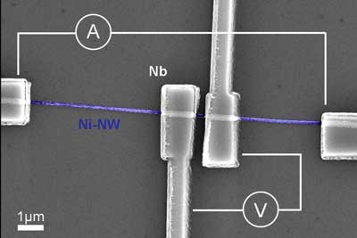 |
| Figure 1. Microscopy image of the studied structure. Superconducting niobium electrodes in the center are shown in gray, while the ferromagnetic nickel nanowire is in blue. The letters A and V (ammeter and voltmeter) indicate the ways in which a current is passed through the sample. (© O. V. Skryabina et al./Scientific Reports) |
| The researchers examined a system consisting of two superconducting niobium electrodes connected by a nickel nanowire (see figure 1 above) and observed that changes in the magnetic field lead to a strong dependence of the nanowire resistance on the phenomena occurring near the superconductor/ferromagnet interface. |
| First, the physicists examined the system in its normal state: when the temperature was above the critical value and the magnetic field uniformly penetrated the sample (figure 2a). Despite the strength of the magnetic field being increased, the resistance of the sample remained relatively unchanged. |
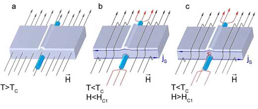 |
| Figure 2. The processes occurring in the niobium (gray block) / nickel nanowire (blue cylinder) system under various ambient conditions. (a) The temperature is above the critical value. The system is in its normal state, the magnetic field (black arrows) uniformly enters the sample. (b) The temperature is below the critical value. When Hc < H < Hc1, the magnetic field is concentrated in the ferromagnetic nanowire (red arrows) and is screened by niobium (black arrows). (c) T < Tc, when the applied field exceeds the first critical field H > Hc1, an Abrikosov vortex penetrates niobium (marked by a red circle). (© O. V. Skryabina et al./Scientific Reports) |
| Next, the researchers cooled the temperature below the critical value. The niobium electrodes underwent a transition to the superconducting state, their resistance dropping to zero. At the same time, a substantial rise in the resistance of the system was registered. This can only be explained by the fact that the edge regions contributed to the resistance. |
| Meanwhile, screening currents began to circulate in the niobium electrodes, and the superconductor began to expel the magnetic field (figure 2b). This resulted in an unusual behavior in the magnetoresistance signal (saw-shaped curves) and a shift relative to various magnetic field sweeps (figure 3). |
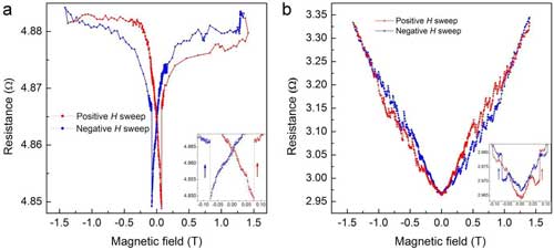 |
| Figure 3. The resistance of the sample as a function of the applied magnetic field. The blue and red colors correspond to different magnetic field sweep directions. (a) The temperature is above the critical value. The system is in its normal state, the resistance of the system remains largely unchanged (mostly due to the magnetization reversal of the nickel nanowire). (b) The temperature is below the critical transition temperature. The resistance of the system grows rapidly. The curve is saw-shaped and has resistance jumps that correspond to Abrikosov vortex penetration/exit. Subplots are zoomed-in images in the nanowire reversal magnetization range. (© O. V. Skryabina et al./Scientific Reports) |
| “We placed the sample in a magnetic field parallel to the major axis of the nanowire. It turned out that by measuring the resistance of the sample under such conditions we were able to determine when a magnetic flux quantum enters or leaves the superconducting electrode,” says Olga Skryabina. |
| This penetration/escape of individual vortices into/from niobium accounts for the mentioned saw-like electrical resistance behavior (figure 2c). The nickel nanowire in the system serves as a lightning rod, “attracting” the magnetic field. The contact with it weakens the superconductivity of the niobium electrodes and thus determines the regions from which the vortices can penetrate. |
| The study shows a striking difference between conventional electric circuits and superconducting ones. It also indicates a need for more detailed research into hybrid superconducting devices for the purpose of developing more advanced superconducting digital and quantum computers as well as highly sensitive sensors. |
| Source: Moscow Institute of Physics and Technology |
|
Subscribe to a free copy of one of our daily Nanowerk Newsletter Email Digests with a compilation of all of the day's news. |

