| Apr 20, 2020 |
New 'brick' for nanotechnology: Graphene Nanomesh(Nanowerk News) Researchers at Japan Advanced Institute of Science and Technology (JAIST) have successfully demonstrated the fabrication of large-area suspended graphene nanomesh (GNM) by helium ion beam microscopy. The team uniformly patterned 6 nm diameter nanopores were patterned on 1.2 µm long and 500 nm wide suspended graphene. |
| By systematically controlling the pitch (nanopore’s center to nanopore’s center) from 15 nm to 50 nm, a series of stable graphene nanomesh devices were achieved. |
| This provides a practical way to investigate the intrinsic properties of graphene nanomesh towards the application for gas sensing, phonon engineering, and quantum technology. |
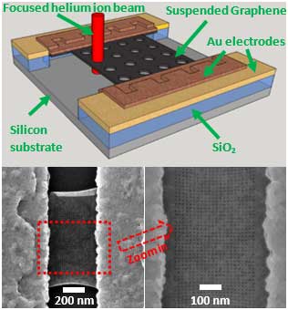 |
| Top: Schematic illustration of the 3D structure of the suspended GNM device. The Au electrodes on the two sides were used to apply drain voltage (VD) and source voltage (VS). The silicon substrate at the bottom was used to apply back gate voltage (VBG). Bottom: (a) HIB secondary electron microscopy image of typical suspended GNM devices. (b) 6 nm diameter nanopores and missing nanopores by zooming in at (a). (Image: JAIST) |
| Graphene, with its excellent electrical, thermal and optical properties, is promising for many applications in the next decade. It is also a potential candidate instead of silicon to build the next generation of electrical circuits. However, without a bandgap, it is not straightforward to use graphene as field-effect transistors (FETs). |
| Researchers tried to cut the graphene sheet into a small piece of graphene nanoribbon and observed the bandgap opening successfully. However, the current of graphene nanoribbons is too low to drive the integrated circuit. In this case, the graphene nanomesh is pointed out by introducing periodical nanopores on the graphene, which is also considered as very small graphene nanoribbon array. |
| A research team led by Dr Fayong Liu and Professor Hiroshi MIZUTA has demonstrated in collaboration with researchers at the National Institute of Advanced Industrial Science and Technology (AIST) that large area suspended graphene nanomesh is quickly achievable by helium ion beam microscopy with sub-10 nm nanopore diameter and well-controlled pitches (Micromachines, "Conductance Tunable Suspended Graphene Nanomesh by Helium Ion Beam Milling"). |
| Compared to slow speed TEM patterning, the helium ion beam milling technique overcomes the speed limitation while providing high imaging resolution. With the initial electrical measurements, the researchers found that the thermal activation energy of the graphene nanomesh increased exponentially with increasing porosity of the graphene nanomesh. This immediately provides a new method for bandgap engineering beyond the conventional nanoribbon method. The team plans to continue exploring graphene nanomesh towards the application of phonon engineering. |
| “Graphene nanomesh is a kind of new ‘brick’ for modern micromachine systems. Theoretically, we can generate many kinds of periodical patterns on the original suspended graphene, which tunes the property of the device to the direction for a special application, in particular nanoscale thermal management” says Prof. Hiroshi Mizuta, the Head of Mizuta Lab. |
| The Mizuta lab is currently developing the electrical and thermal properties of graphene-based devices for fundamental physics and potential applications such as gas sensors and thermal rectifiers. |
| Source: Japan Advanced Institute of Science and Technology |
|
Subscribe to a free copy of one of our daily Nanowerk Newsletter Email Digests with a compilation of all of the day's news. |

