| Jul 14, 2020 |
Exchange bias in van der Waals heterostructures(Nanowerk News) National University of Singapore (NUS) scientists have discovered the exchange bias phenomenon in van der Waals CrCl3/Fe3GeTe2 heterostructures (Nano Letters, "Exchange Bias in van der Waals CrCl3/Fe3GeTe2 Heterostructures"). |
| This phenomenon has a number of applications in magnetic sensors and magnetic reading heads, which, however, have not been reported in van der Waals heterostructures before. |
| The exchange bias effect manifests itself as a shift of the hysteresis loop to the negative or positive direction with respect to the applied field. The mechanism is generally ascribed to a unidirectional pinning of a ferromagnet (FM) by an adjacent antiferromagnet (AF). |
| Therefore, compared to a single ferromagnet (free layer) without such a unidirectional pinning, a properly designed exchange-biased AF/FM system (pinned layer) has a preferred magnetisation direction and a relatively high switching field. |
| Thus, a device comprising one pinned and one free layer, with a spacer, may serve as a sensor for the direction and strength of the magnetic field. The device will have two distinct memory states (“1” and “0”) defined by the magnetisation in the free layer, either parallel or antiparallel to the pinned layer. |
| Such a device, well known as spin valves and magnetic tunnel junctions, are being widely embedded in memory technologies such as storage media, readout sensors, and magnetic random access memory. |
| The exchange bias effect has been replicated in a broad range of AF/FM interfaces, for example, the IrMn/NiFe metal bilayers widely used in commercial read heads. If these AF/FM bilayer systems are made of magnetic van der Waals heterostructures that exhibit exchange bias effect, it could be beneficial for the devices to potentially approach atomically thin dimensions and be more flexible. |
| A team led by Prof Andrew WEE, Department of Physics and Centre for Advanced 2D Materials, NUS, has discovered the presence of the exchange bias effect in mechanically exfoliated CrCl3/Fe3GeTe2, a van der Waals heterostructure. |
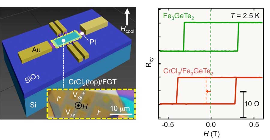 |
| Schematic showing (left) the device structure, with optical image of the CrCl3/Fe3GeTe2 heterostructure on top of the Pt Hall contacts shown in the inset. (Right) Rxy~H loops showing the experimental outcome of the tests done on the device structure using two types of materials – individual Fe3GeTe2(30 nm) and CrCl3(15 nm)/Fe3GeTe2(30 nm) heterostructure, both measured at a temperature of 2.5 K. The plot for Fe3GeTe2 (top panel) is symmetric with respect to the zero point along the H-axis. In contrast, the plot for the CrCl3/Fe3GeTe2 heterostructure (bottom panel) shifts to the left, indicating an exchange bias. (© Nano Letters) (click on image to enlarge) |
| The researchers fabricated a test device by transferring thin flakes of CrCl3 and Fe3GeTe2 onto a SiO2/Si substrate. The measured value of the biased field for the test device is over 50 mT (at a temperature of 2.5 K). |
| This is comparable to reported values in conventional exchange biased AF/FM metallic multilayers. Moreover, the biased field is highly tunable and can be adjusted by changing the field-cooling process and the thickness of the heterostructure. The research team also proposed a theoretical model explaining that the spin configurations in CrCl3 plays a crucial role in the exchange bias effect in the heterostructure. |
| “Our observation is of immense importance since it validates the existence of the exchange bias effect in a 2D van der Waals interface, which addresses a key issue in the 2D research community,” said Prof Wee. |
| The work is a collaboration with Prof ZHANG Wen from Northwestern Polytechnical University, China (a former research fellow in Prof Wee’s group) and Prof ZHAI Ya from Southeast University, China. |
| Next, the team aims to incorporate such heterostructures into functional flexible devices, with a greatly reduced thickness and an increased working temperature. |
| Source: National University of Singapore |
|
Subscribe to a free copy of one of our daily Nanowerk Newsletter Email Digests with a compilation of all of the day's news. |

