| Mar 09, 2021 |
Integration of 2D materials on silicon Mie resonators for electrically controlled nanopixels(Nanowerk News) Nanopixels that are thousands of times smaller than those in commercial CMOS image sensors have drawn great attention because of the potential applications for the miniaturization of photonic and optoelectronic devices. To build nanopixels, sub-wavelength light localization and electrical tuning are important foundations. |
| All-dielectric (e.g. silicon) nanostructures have emerged as modern building blocks in nanophotonics, which help to overcome the high level of Joule losses in metallic plasmonic nanostructures. From the intense magnetic dipole resonances based on the Mie theory to the toroidal mode and anapole mode, the unique resonant modes of all-dielectric nanostructures offer a variety of intriguing optical effects. |
| However, the indirect band gap of silicon limits the optoelectronic performances. |
| The emerging of 2D materials makes it possible for hybrid integration with CMOS-compatible silicon nanostructures to enhance the optoelectronic performances. Specially, the electromechanical properties of 2D materials considerably influence and render an innovative perspective to the electrically tunable nanopixels. |
| Reporting in Advanced Optical Materials ("Individual Si nanospheres wrapped in a suspended monolayer WS2 for electromechanically controlled Mie-type nanopixels") featured as front cover, Dr. Jiahao Yan and co-authors in Jinan University, China develop Si-WS2 hybrid nanopixels with electromechanically controlled Mie-exciton optical responses with high modulation depth. |
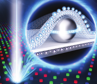 |
| Schematic diagram of the nanopixel based on a single Si nanosphere covered by a suspended WS2 monolayer. (© Wiley-VCH Verlag) |
| The proposed nanopixel is based on a single Si nanosphere covered by a suspended WS2 monolayer as the umbrella shape, which effectively overlap with the Mie resonant field distributions on the surfaces of Si nanospheres. |
| Therefore, the electrically induced displacement of WS2 monolayers within a few nanometers influences the near-field distributions of Si nanospheres and changes the overall optical responses. |
| In experiments, electromechanical tuning of the dark-field scattering with 40% attenuation and photoluminescence with 0.014 eV peak shift were demonstrated. |
| “We hope,” Dr. Yan said, “the proposed electromechanically controlled hybrid nanopixels will give a new insight on the design of optoelectronic devices at a subwavelength level and contribute to the on-chip nanoscale optical interconnections.” |
| Source: Jinan University |

