| Aug 03, 2022 |
Enhancing solar efficiency with upconversion(Nanowerk News) Solar cell technologies have been improving incrementally over the decades, but energy conversion has remained less than optimal. |
| Now, researchers at Kyoto University have developed a novel wafer bonding technology using an optical upconversion material that transforms sunlight to shorter-wavelengths. This new semiconductor process utilizes the interface's optical function for bond formation (Applied Physics Letters, "Upconversion semiconductor interfaces by wafer bonding for photovoltaic applications"). |
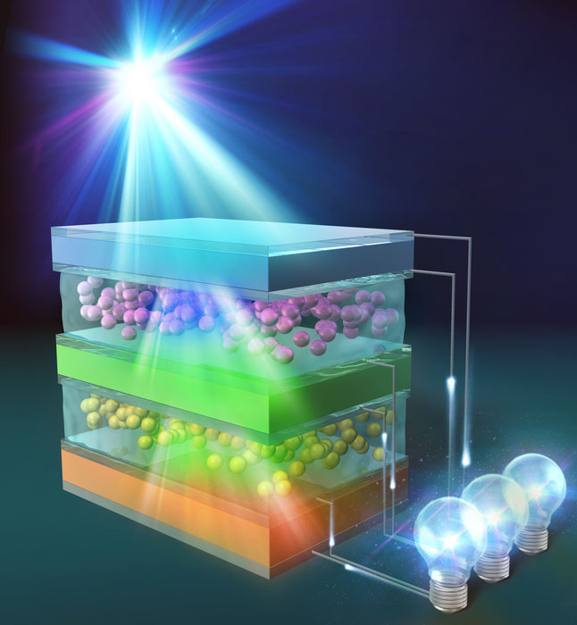 |
| Semiconductor bonding mediated by upconversion material. (Image: Katsuaki Tanabe, Kyoto University) |
| The team created a stacked structure consisting of a thin silicon film mimicking the upper subcell of a multi-junction solar cell and a silicon solar cell wafer; these layers were bonded with an adhesive made from upconversion nanoparticles dispersed in a hydrogel. |
| Conventional multi-junction solar cells are created with the vapor phase growth method. However, this method is limited by lattice matching in semiconductor materials. |
| The team, led by Katsuaki Tanabe, has applied their wafer bonding method to the production of a range of optical and electronic devices, demonstrating that different semiconductor materials can be stacked in any combination without the restriction of lattice matching. |
| "Even inherently non-absorbed light of longer wavelengths in the lower subcell of a multi-junction solar cell could be used to enhance the efficiency of the overall energy conversion via our upconverting interface," concludes the author. |
| Source: Kyoto University |

