| Nov 29, 2023 |
Applying semiconductor manufacturing principles to optoelectronic devices
(Nanowerk News) Optoelectronics detect or emit light and are used in a variety of devices in many different industries. These devices have historically relied on thin transistors, which are small semiconductors that control the movement of electrons and photons, made out of graphene and other two-dimensional materials. However, graphene and these other materials often have problems with band gap opening and other shortcomings that have researchers searching for an alternative.
|
|
When treated with a method called the Lewis acid treatment, palladium diselenide is a possible solution to satisfy the needs of optoelectronic devices.
|
Key Takeaways |
|
Optoelectronic devices, historically reliant on graphene and similar materials, face challenges with band gap opening, prompting the exploration of alternatives.
Palladium diselenide emerges as a promising solution, displaying unique properties like a tunable band gap and high performance, particularly after Lewis acid treatment.
Doping palladium diselenide with tin chloride through Lewis acid treatment alters its energy bandgap, enhancing the material's suitability for optoelectronic applications.
Research confirms the feasibility of controlling palladium diselenide's threshold voltage by varying tin chloride concentration, guiding future doping approaches.
Future research aims to scale these methods for industrial application in electronic components and smart biomedical systems for healthcare monitoring.
|
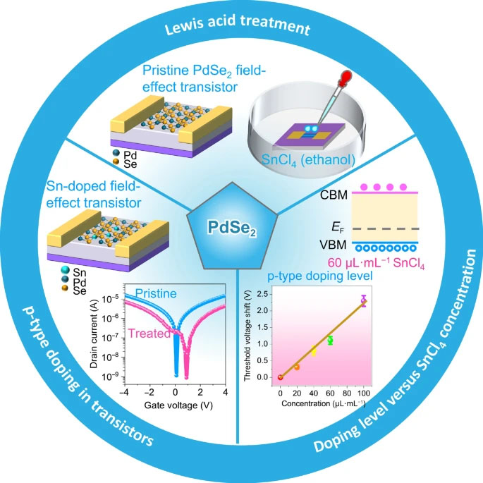 |
| This graphic shows how the Lewis acid treatment, p-type doping, and tin chloride concentrations and their effects on palladium diselenide, used in transistors for optoelectronic devices. (© Nano Research, Tsinghua University Press)
|
The Research |
|
Research analyzing this method was published in a paper in Nano Research ("Modulating p type doping of two dimensional material palladium diselenide").
|
|
Prof. Dr. Mark H. Rümmeli, ERA Chairs professor at the Technical University of Ostrava (VSB-TUO) stated, "Palladium diselenide exhibits unique physical properties, including a tunable band gap and impressive device performance. Notably, it demonstrates long-term stability in ambient air without the need for additional packaging."
|
|
Taking inspiration from semiconductor physics, the researchers considered how doping might alter palladium diselenide to improve its performance. Doping is the intentional introduction of impurities to a material, resulting in three types of materials: pristine, p-type doped, and n-type doped. When a p-type doped material and an n-type doped material touch, they create a p-n junction. This junction is important for optoelectronic devices, because it is where light to electron and electron to light conversion occurs.
|
|
To create p-type doped and n-type doped palladium diselenide in a controlled fashion, researchers used the Lewis acid treatment. “The controlled level of doping can make palladium diselenide have a different energy bandgap, which enriches a toolkit or library of materials for the selection and design of the p-n junction,” said Dr. Hong Liu, a professor at the State Key Laboratory of Crystal Materials at Shandong University in Jinan China. “The Lewis acid treatment can introduce the substitution of the palladium atoms (by tin from tin chloride, one type of Lewis acid) in the palladium diselenide. We found a data fitting equation between the doping level versus the concentration of Lewis acid, which may inspire people to manipulate more p-type doped two dimensional materials.”
|
|
In order to test this method, researchers prepared a pristine film of palladium diselenide. The film was then modified using the Lewis acid treatment. After the initial Lewis acid treatment, the lattice structure of the palladium diselenide film was unchanged, but emerging peaks of tin, palladium, and selenium were confirmed using imaging. These peaks proved that tin could be used as a p-type dopant.
|
|
Additional tests of different concentrations of tin chloride showed how the threshold voltage of the palladium diselenide could be controlled depending on the concentration of the tin chloride. These guidelines can be applied for future doping of palladium diselenide using Lewis acids. It could also provide a blueprint for how to do similar testing on other semiconductor materials.
|
|
Looking ahead, researchers will plan how to scale the processing of these two-dimensional materials. “We will demonstrate the exciting applications of p-type doped palladium diselenide in several electronic components, such as field-effect transistors, photodetectors, and light emitters. We plan to try to optimize the semiconductor doping method, which can be readily adopted by the industrial standards and could be employed in the semiconductor industry for mass production in the near future. Our ultimate goal is to apply this technique in wearable and flexible electronics by integrating the palladium diselenide-based transistors and photodetectors with polymer-based strain sensors in flexible substrates, which result in a smart biomedical system for human healthcare monitoring applications,” said Dr. Jinbo Pang, a professor of chemistry and materials science at the University of Jinan in Jinan, China.
|

