| Feb 27, 2024 |
Grayscale nanolithography for 2D nanoelectronics(Nanowerk News) Grayscale structured surfaces with nanometer-scale features are used in a growing number of applications in optics and fluidics. Thermal scanning probe lithography achieves a lateral resolution below 10 nm and a vertical resolution below 1 nm, but its maximum depth in polymers is limited. |
| Now, researchers in the LMIS1, led by Jürgen Brugger, have developed an innovative combination of nanowriting in thermal resist and plasma dry etching with substrate cooling. |
| Their method, recently published in the journal Microsystems & Nanoengineering ("Combining thermal scanning probe lithography and dry etching for grayscale nanopattern amplification"), achieves up to 10-fold amplification of polymer nanopatterns into silicon dioxide (SiO2) without proportionally increasing surface roughness. |
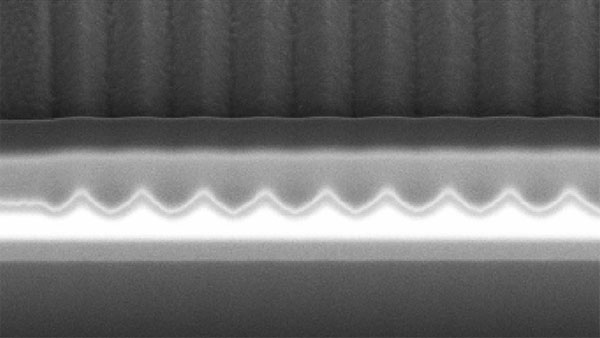 |
| Researchers have published an innovative grayscale nanolithography technique that has potential applications in photonic and nanoelectronic device fabrication. (Image: Microsystems Laboratory in the School of Engineering, EPFL) |
| Sinusoidal nanopatterns in SiO2 with 400 nm pitch and 150 nm depth are fabricated free of shape distortion after dry etching. |
| To exemplify the possible applications of the proposed method, grayscale dielectric nanostructures are used for scalable manufacturing through nanoimprint lithography and for strain nanoengineering of 2D materials. |
| Such a method for aspect ratio amplification and smooth grayscale nanopatterning has the potential to find application in the fabrication of photonic and nanoelectronic devices. |
| Source: By Celia Luterbacher, EPFL (Note: Content may be edited for style and length) |

