Nanoengineering
Nanoengineering is a branch of engineering that deals with all aspects of the design, building, and use of engines, machines, and structures on the nanoscale. At its core, nanoengineering deals with nanomaterials and how they interact to make useful materials, structures, devices and systems.
Nanoengineering is not exactly a new science, but, rather, an enabling technology with applications in most industries from electronics, to energy, medicine, and biotechnology.
While the term nanoengineering is often used synonymously with the more general term nanotechnology, the former technically focuses more closely on the engineering aspects of the field, as opposed to the broader science and general technology aspects that are encompassed by the latter.
Other closely related terms used in this context are nanofabrication and nanomanufacturing. One possible approach to distinguish between the terms is by using the criterion of economic viability: The connotations of industrial scale and profitability associated with the word manufacturing imply that nanomanufacturing is an economic activity with industrial production facilities with more or less fully automated assembly lines. By contrast, nanofabrication is more of a research activity based on developing new materials and processes – it's more a domain of skilled craftsmen and not of mass production.
In general, engineering is the branch of science and technology concerned with the design, building, and use of engines, machines, and structures. Correspondingly, but at the scale of atoms and molecules, nanoengineeering exploit the unique properties of nanoscale materials (size and quantum effects) in order to design and manufacture devices and systems that possess entirely new functionality and capabilities.
The properties of materials can be different at the nanoscale for two main reasons:
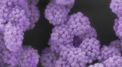
First, nanomaterials have a relatively larger surface area when compared to the same mass of material produced in a larger form. This can make materials more chemically reactive (in some cases materials that are inert in their larger form are reactive when produced in their nanoscale form), and affect their strength or electrical properties.
Second, quantum effects can begin to dominate the behavior of matter at the nanoscale – particularly at the lower end – affecting the optical, electrical and magnetic behavior of materials. Materials can be produced that are nanoscale in one dimension (for example, nanowires, nanorods and nanotubes), in two dimensions (plate-like shapes like nanocoatings, nanolayers, and graphene) or in all three dimensions (for example, nanoparticles).
Nanoscale objects are difficult to manipulate, as they are too tiny to see directly by eye, far too small to hold, and often have incompatible surfaces for assembling into ordered structures. Therefore the fabrication of complex nanoarchitectures requires sophisticated techniques of nanoscale engineering. To do this, nanoengineers are employing a number of methods to leverage the manipulation of materials on an atomic and molecular scale for (ultimately) industrial purposes.
Among the many challenges that researchers have to overcome in developing nanoengineering techniques and processes, the requirement for extremely precise, nanometer-scale control of positioning and shaping of objects is one of the most vexing.
Nanopatterning and nanostructuring of surfaces
There are different ways of fabricating functional nanostructures that you hear most about: top-down and bottom-up methods.
Top-down nanofabrication predominantly is done by photolithography, which is the standard workhorse employed in today's semiconductor industry, and other top-down methods where you start by taking a block of material and remove the bits and pieces you don't want until you get the shape and size you do want.
In contrast to the deterministic nature of top-down processes, bottom-up processes are driven by a combination of thermodynamics and kinetics, which then determines the yield of the desired structure.
Bottom-up processes typically don't need expensive tooling to create nanoscale structures, and scaling to large volumes is potentially straightforward. With the application of the tools of chemical synthesis, quantum dots, plasmonically active particles, carbon nanotubes, metallic nanowires, and multifunctional particles for medical applications have been successfully produced in manufacturing quantities.
Given the vast, and still rising, cost of optical lithography tools, researchers have considered alternative patterning technologies such as electron beam lithography (EBL), and nanoimprint technology (NIL) in order to enable the manufacturing of next-generation integrated circuits, flash memory, and hard disk drives.
Now that the length scales attainable by top-down lithography are approaching that of bottom-up self-assembly found in polymers and small molecules, scientists are increasingly looking at bottom-up patterning technologies based on self-assembly.
The utilization of organic building blocks as self-assembled etch masks is particularly attractive since the lithographic information is contained in the self-assembling material itself, rather than provided in an exposure step.
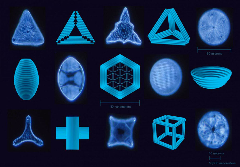
Architecture is key when designing new materials and DNA is probably the most programmable biomaterial for creating a wide range of rationally designed and functionally enhanced nanostructures.
DNA nanotechnology employs DNA as a programmable building material for self-assembled, nanoscale structures with precisely controlled structures, that can lead to improved surface properties relevant to biosensing, materials science, and cell biology.
3D printing
Fabrication of three-dimensional (3D) objects through direct deposition of functional materials – also called additive manufacturing – has been a subject of intense study in the area of macroscale manufacturing for several decades. These 3D printing techniques are reaching a stage where desired products and structures can be made independent of the complexity of their shapes – even bioprinting tissue is now in the realm of the possible.
Applying 3D printing concepts to nanotechnology could bring similar advantages to nanoengineering – speed, less waste, economic viability – than it is expected to bring to manufacturing technologies.
In addition, pre-patterned micro- or nanostructures could be used as substrates, allowing researchers to realize unprecedented manufacturing flexibility, functionality and complexity at the nanoscale.
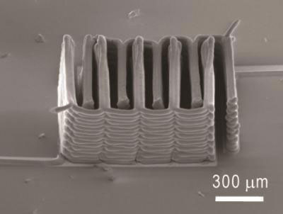
Already, 3D printing can now be used to print lithium-ion microbatteries the size of a grain of sand. To make the microbatteries, a team based at Harvard University and the University of Illinois at Urbana-Champaign printed precisely interlaced stacks of tiny battery electrodes, each less than the width of a human hair.
There are various approaches to 3D nanoprinting. In one, researchers use a novel nanoscale additive manufacturing technique termed Nanotribological Printing, which creates structures through tribomechanical and tribochemical surface interactions at the contact between a substrate and an atomic force microscope probe, where material pattern formation is driven by normal and shear contact stresses.
Another technique has been developed exploiting a size-controllable liquid meniscus to engineer 3D printed nanostructures composed entirely of graphene.
For instance, printing three-dimensional objects with incredibly fine details is already possible using a direct laser writing method called two-photon lithography (read more: "3D-printer with nanoscale precision"). With this technology, tiny structures on a nanometer scale can be fabricated such as the example of the race car – which measures only 285 µm in length.
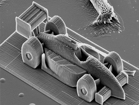
The entire process can be seen here in this video: A race car with dimensions of 330x130x100 µm3 is fabricated. The structure consists of 100 layers, each made of an average of 200 polymer lines. It is finished in 4 minutes and resembles the CAD file at a precision of ±1 µm:
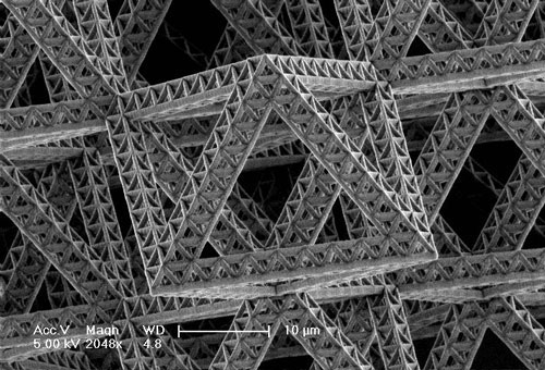
Another example of two-photon lithography is the fabrication of elaborate fractal truss micro- and nanostructures such as the one below. Here, a pattern in a polymer, allowing a laser beam to crosslink and harden the polymer wherever it is focused. In contrast to a 3D-printing-only process, though, this technique requires additional steps such as coating the scaffold and etching out unused polymer.
 By
Michael
Berger
– Michael is author of four books by the Royal Society of Chemistry:
Nano-Society: Pushing the Boundaries of Technology (2009),
Nanotechnology: The Future is Tiny (2016),
Nanoengineering: The Skills and Tools Making Technology Invisible (2019), and
Waste not! How Nanotechnologies Can Increase Efficiencies Throughout Society (2025)
Copyright ©
Nanowerk LLC
By
Michael
Berger
– Michael is author of four books by the Royal Society of Chemistry:
Nano-Society: Pushing the Boundaries of Technology (2009),
Nanotechnology: The Future is Tiny (2016),
Nanoengineering: The Skills and Tools Making Technology Invisible (2019), and
Waste not! How Nanotechnologies Can Increase Efficiencies Throughout Society (2025)
Copyright ©
Nanowerk LLC
