| Oct 21, 2011 |
New wafer-level MEMS packaging technology using nanoporous alumina membranes |
| (Nanowerk News) Imec engineers have, for the first time, demonstrated the fabrication of extremely small sealed cavities (less than one picoliter in volume), fabricated directly on 200mm silicon wafers. The crucial process step is the production of freestanding thin membranes of nanoporous anodic alumina (PAA). Used for wafer-level packaging of MEMS, the thin-film vacuum technology results in strong and air-tight packages. The process is simple, low-temperature, non-organic, and RF-compatible. The packages have a negligible impact on RF transmission, and tests show good results for package hermeticity. |
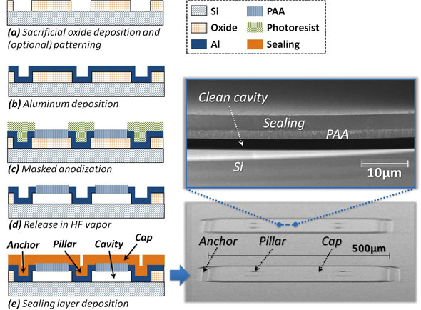 |
| Scanning electron microscopy (SEM) pictures of the fabricated empty PAA-based thin-film packages, together with cross-section schematics (a-e) showing the process steps to produce such structures. |
| Wafer-level packaging of MEMS is essential to protect the fragile MEMS structures from the hazards of back-end assembly and from the operating environment. But conventional thin-film technology has a high process complexity. Also, to remove the sacrificial layer and to form the microcavity between the MEMS and the capping layer, lithography-defined release holes or channels have to be made. These add the risk that sealing material leaks inside the cavity and onto the MEMS structures. |
| To overcome this risk, the new method uses a cap layer with nanopores. This cap layer is a freestanding PAA membrane with a thickness of 2-3µm. The cylindrical nanopores are a mere 15-20nm in diameter, which results in an aspect ratio of >100. The nanopores serve as release etch holes. But because of their high aspect ratio, these holes close very rapidly during the first stage of the sealing, so that no sealing material leaks into the cavity underneath. |
| Schematically, the new process flow has the following steps. First a 3µm chemical vapor deposition (CVD) oxide sacrificial layer is deposited, which is patterned to obtain anchors and supporting pillars for the package. Next, a 1-1.5µm aluminium layer is sputtered. This layer is then anodized, using a mask to define the areas where the microcavities should be made. This results in PAA membranes which are typically 50% thicker than the original aluminium layer. Next, the sacrificial oxide layer under the membranes is etched away by exposing the wafer to HF vapour. And last, the packages are sealed using a 4µm plasma-enhanced CVD (PECVD) silicon nitride layer. This yields relatively strong dielectric caps with a negligible impact on the RF characteristics for signal frequencies up to 67GHz. Also, the dielectric caps are optically transparent, which is useful for optical MEMS applications. |
| Source: imec |

