| Jun 09, 2012 |
New nanomaterials method for boosting computer speed and improving memory density
|
|
(Nanowerk News) When searching for the technology to boost computer speeds and improve memory density, the best things come in the smallest packages.
|
|
A relentless move toward smaller and more precisely defined semiconductors has prompted researchers at the U.S. Department of Energy's (DOE) Argonne National Laboratory to develop a new technique that can dramatically improve the efficiency and reduce the cost of preparing different classes of semiconducting materials (see paper in Advanced Materials: "Enhanced Lithographic Imaging Layer Meets Semiconductor Manufacturing Specification a Decade Early").
|
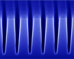 |
| This image shows channels etched using sequential infiltration synthesis, which scientists at Argonne have used to create features that have high aspect ratios – that is, they are far deeper than wide. These crevasses will permit the creation of a new generation of semiconducting materials.
|
|
The new discovery meets certain requirements of the international semiconductor "roadmap" all the way out to 2022—leapfrogging an anticipated ten years of progress with a single set of experiments.
|
|
Most semiconductor patterns are currently made using a process known as photolithography, in which portions of a thin film are selectively removed to create a pattern. The pattern in this film, known as a resist, is etched into the semiconductor by exposure to an ionized gas. This gas also etches away the resist itself, reducing the number of times the film can be used. Especially durable resists are known as hard masks.
|
|
The drive to create smaller and smaller semiconductor components is often limited by a phenomenon known as domain collapse, said Argonne nanoscientist Seth Darling. Conventional lithography -- the technique used to make patterns in materials -- attempts to create features that are separated like the teeth of a comb. However, gaps in the resist that are too deep tend to collapse inwards, which makes the material useless.
|
|
"Engineers have tried many ways of avoiding this collapse, but the industry is constantly running up against it," Darling said.
|
|
In 2010, Darling and his colleagues developed a technique known as sequential infiltration synthesis (SIS), which used gases to grow hard inorganic materials inside a soft polymer film. The work was supported by the DOE Office of Science through Argonne's Center for Nanoscale Materials and the Argonne-Northwestern Solar Energy Research Center.
|
|
One of the most notable benefits of SIS is that it eliminates the need for hard masks in photolithography, according to Darling. "Hard masks are a real pain when it comes to semiconductor processing – they're expensive, complicated, reduce pattern quality and add extra steps," he said.
|
|
According to Darling, sequential infiltration synthesis has already been identified by leading semiconductor companies as a technology with the potential to overcome several different limitations.
|
|
In a recent experiment, Darling and his Argonne colleagues showed that SIS can actually eliminate pattern collapse, enabling the fabrication of materials that have patterns with higher "aspect ratios," which measures the height of a feature divided by its width.
|
|
Generally speaking, lithography seeks to create patterns with higher aspect ratios while using as little resist as possible. "Usually, you need a certain thickness of the resist in order for the process to work," Darling said. "This new process enables us to do away with a lot of that problem."
|
|
"One of the biggest advantages of this new study is that we've shown the possibility of using SIS for photolithography, which is one of the most industrially important processes," Darling said. "As there's more and more demand for better electronics, the sizes of these semiconductors need to keep getting smaller and smaller, and it becomes that much more important for us to meet and exceed the benchmarks that we've set for ourselves."
|

