Showing Spotlights 65 - 72 of 254 in category All (newest first):
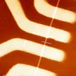 The advent of graphene resulted in a massive, world-wide, effort directed at investigation of other two-dimensional (2D) layered materials. One-dimensional (1D) bundled materials have received considerably less attention. Similar to the 2D layered materials with covalently bonded layers separated by the van der Waals gaps, the 1D materials consist of covalently bonded one-dimensional wires with van der Waals gaps between the wires. Researchers now have discovered that quasi-1D nanoribbons reveal an exceptionally high current density at the peak of the stressing DC current. This level of the current density exceeds that in any conventional metals like copper by almost two orders of magnitude.
Apr 19th, 2018
 Sensory substitution with flexible electronics is one of the intriguing fields of research that takes place in nanotechnology labs around the world. In line with this focus on human senses, in the future artificial retinas integrated with the human body may not only repair damaged vision but also expand it to see a wider range wavelengths (e.g. ultraviolet light). Researchers now have demonstrated a new self-powered brain-linked vision electronic skin (e-skin) for mimicking the human retina. The general idea of our device design of brain-linked vision electronic skin is constructing an integrated flexible system including photodetector array, information analyzer, signal transmitter, and electricity power unit.
Apr 18th, 2018
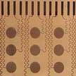
 Next-generation electronic devices will be highly portable, wearable - even transplantable - lightweight, and most likely self-powered. Among the various functional block required for these systems (such as displays, sensors, actuators, etc), some of the most important components are novel flexible data storage systems that possess nonvolatile ability, high-density storage, high-switching speed, and reliable endurance properties. Especially organic memories have been considered as the most promising candidates to be used in various portable and wearable systems in future due to their remarkable advantages of nonvolatile memory features, low cost, easy fabrication, and flexibility.
Apr 9th, 2018
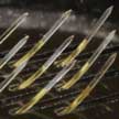 Whiskers on animals allow them to build a rich understanding of their environment by feeling objects or even the flow of fluids. Many animals can also actively sweep, or 'whisk', their whiskers, enabling them to gather complex information about the architecture of their environment. Researchers have replicated this whisking action by exploiting the shape memory effect of a polymer substrate, which can be dynamically repositioned by modulating the temperature and air flow across the electronic whiskers (e-whiskers).
Apr 3rd, 2018
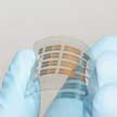
 In new work employing the photostrictive effect, researchers have fabricated a flexible two-dimensional (2D) charge transfer molecular (sub-nanometer) nanosheet and observed a sizeable photostrictive effect of 5.7% with fast, sub-millisecond response; this is higher than that of some conventional ferroelectronics and polar semiconductors. This photostrictive effect arises from excess charge carriers induced lattice dilation and conformation change, which is higher than that of some conventional ferroelectronics and polar semiconductors.
Mar 27th, 2018
 Despite the rise of graphene and other two-dimensional (2-D) materials, semiconducting single-walled carbon nanotubes are still regarded as strong candidates for the next generation of high-performance, ultra-scaled and thin-film transistors as well as for opto-electronic devices. In new work, a European team of researchers demonstrates simultaneous confinement of electrons and holes between artificial defects separated by less than 10 nm in semiconducting carbon nanotubes.
Mar 16th, 2018
 Optics and mesoscopic physics teams have discovered a new cooling mechanism concerning electronic components made of graphene deposited on boron nitride. The efficiency of this mechanism allowed them to reach electric intensities at the intrinsic limit of the laws of conduction. This new mechanism, which exploits the two-dimensional nature of the materials opens a 'thermal bridge' between the graphene sheet and the substrate. Researchers have demonstrated the effectiveness of this mechanism by imposing in graphene levels of electrical current still unexplored, up to the intrinsic limit of the material and without any degradation of the device.
Jan 9th, 2018
 In trying to bring brain-like (neuromorphic) computing closer to reality, researchers have been working on the development of memory resistors, or memristors, which are resistors in a circuit that 'remember' their state even if you lose power. Now, scientists have discovered non-volatile memory effect in atomically thin 2D materials such as MoS2. This effect is similar to memristors or RRAM in metal oxide materials. These devices can be collectively labeled atomristor, in essence, memristor effect in atomically thin nanomaterials or atomic sheets.
Jan 2nd, 2018
 Subscribe to our Nanotechnology Spotlight feed