Dirac Cone in Quantum Materials
Dirac cones, named after the renowned physicist Paul Dirac, are unique features found in the electronic band structures of certain materials, such as graphene and topological insulators. These cones play a vital role in defining the electron transport properties of these materials and have paved the way for a deeper understanding of quantum mechanics.
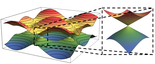
Understanding Dirac Cones
In materials with Dirac cones, the valence and conduction bands take the shape of the upper and lower halves of a conical surface, meeting at points called Dirac points. These points occur at energies near the Fermi level, and they represent the crossing-points in the electronic band structure that electrons avoid. The energy of the valence and conduction bands is not equal anywhere in the two-dimensional lattice k-space, except at the zero-dimensional Dirac points.
Role of Massless Fermions and the Dirac Equation
Due to the presence of Dirac cones, electrical conduction in these materials can be described by the movement of charge carriers, which are massless fermions. The theoretical framework to describe this behavior is provided by the relativistic Dirac equation. These massless fermions give rise to various quantum Hall effects, magnetoelectric effects in topological materials, and ultra-high carrier mobility.
Historical Discoveries and Observations
Dirac cones were first observed in 2008-2009 using angle-resolved photoemission spectroscopy (ARPES) on the potassium-graphite intercalation compound KC8 and several bismuth-based alloys. As a three-dimensional object, Dirac cones are a feature of two-dimensional materials or surface states, characterized by a linear dispersion relation between energy and the two components of the crystal momentum, kx and ky.
Extending the Concept: Dirac Semimetals and Weyl Semimetals
The concept of Dirac cones can be extended to three dimensions, where Dirac semimetals are defined by a linear dispersion relation between energy and kx, ky, and kz. In k-space, this results in a hypercone with doubly degenerate bands meeting at Dirac points. Dirac semimetals contain both time reversal and spatial inversion symmetry. When one of these symmetries is broken, the Dirac points split into two constituent Weyl points, and the material transitions into a Weyl semimetal. In 2014, the Dirac semimetal band structure was directly observed using ARPES on the Dirac semimetal cadmium arsenide.
Conclusion
Dirac cones have emerged as a fascinating and essential feature in the study of quantum materials like graphene and topological insulators. These unique structures have provided invaluable insights into the electron transport properties of these materials, and have led to exciting discoveries in the field of quantum mechanics. As our understanding of Dirac cones and related materials continues to grow, so too will our ability to harness their unique properties for applications in advanced technologies.
Further Reading
ChemPhysMater, Two-dimensional Dirac materials: Tight-binding lattice models and material candidates
Light: Science & Applications , Dirac-like cone-based electromagnetic zero-index metamaterials
Physical Review B, Measuring Dirac cones in a brick-wall lattice microwave metamaterial
Check out these latest Nanowerk News:


