| Posted: Jul 23, 2009 |
Integrating nanotube-based NEMS into large scale MEMS |
| (Nanowerk Spotlight) The fundamental issue of large-scale carbon nanotube (CNT) device fabrication remains the biggest challenge for effective commercialization of CNT-based nanoelectronic devices. For CNT electronics to become a reality requires manufacturing techniques to simultaneously and reproducibly fabricate a very large number of such devices on a single chip, each accessible individually for electronic transport. Conventional nanotube growth and device fabrication techniques using chemical vapor deposition or spin-casting are unable to achieve this, due to a lack of precise control over nanotube positioning and orientation. |
| Researchers are working on exciting projects – for instance through dielectrophoretic deposition of CNTs (see "Carbon nanotubes to the rescue of Moore's law") – to bring CNT electronics closer to reality. Another recent example is a chemical vapor deposition (CVD) CNT growth method developed in Israel to achieve the integration of carbon nanotubes into micro-fabricated devices. |
| "Past studies demonstrated integration of suspended single-walled CNT into silicon based devices," Yael Hanein tells Nanowerk. "However, fabrication processes needed in order to place the tubes in the right place and to electrically contact them are not compatible with simple fabrication procedure commonly employed by the industry. We were motivated by the need to develop a simple method to integrate taut carbon nanotubes with standard micro-fabrication processes." |
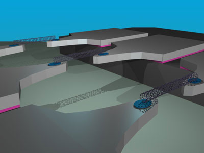 |
| Schematic representation of CNTs bridging neighboring pillars. (Image: Dr. Hanein, Tel Aviv University) |
| Hanein is a senior lecturer at Tel Aviv University and a member of the university's Center for Nanoscience and Nanotechnology. The research in her group is focused on developing novel micro and nanofabrication techniques and systems. Previously, we have reported on her group's technique for making complex networks of carbon nanotubes that can be stamped onto circuit boards. The scientific core of her new work is the complex dynamics of carbon nanotubes during chemical vapor deposition growth. |
| "By understanding the mechanisms governing carbon nanotube growth and by exploiting their interactions with various surfaces, we were able to grow well aligned electrically-contacted single wall carbon nanotubes," she says. "The ability of carbon nanotubes to grow at specific positions pending proper chemical and mechanical design of the micro-fabricated device offer a simple approach to form devices which otherwise require very cumbersome fabrication approaches." |
| The team – which included Slava Krylov, a senior lecturer at the Department of Mechanical Engineering at Tel-Aviv University and graduate students Gabriel Karp, Assaf Ya'akobovitz, and Moshe David-Pur – utilizes the CVD growth of CNTs over pillar-patterned silicon substrates to facilitate the formation of devices with taut and aligned CNTs grown exclusively at desired positions with built-in electrical contacts. |
| "Our approach builds on common silicon-on-insulator microfabrication techniques combined with conventional thermal CVD of CNTs," explains Hanein. "We exploit the selectivity of CNT growth on different substrates – i.e. silicon versus oxidized silicon – to confine the CNT growth to particular locations. The interaction between the CNTs and the silicon surface affects the tube alignment and tautness. We circumvent the poor compatibility of many conducting materials with the CVD growth process by positioning the electrode material next to the growth site rather than directly under it. The contact between the electrode and the tubes is obtained as a result of the tube interaction with the device surfaces." |
| Hanein points out that they were specifically looking for a method which can be implemented in a manufacturing environment. Therefore, any approach relying on intensive manual work had to be ruled out. |
| "We decided instead to exploit the mechanisms that affect carbon nanotube growth to do the work for us. Specifically, by using the CNT's sensitivity to different materials and surfaces during the growth, a simple method to integrate suspended, taut and defect-free carbon nanotubes into complex devices became feasible." |
| One restriction of this technique currently is the inability to control the chirality of the CNTs. This results in great variations of the electrical properties of the tethered nanotubes. The scientists feel confident, though, that the variability between CNT devices can readily be overcome during the testing stage. "In fact" says Hanein, "Raman spectroscopy can readily be implemented to characterize the tubes and to identify their metallic or semi-conducting properties." |
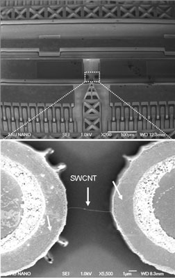 |
| A test MEMS device with a single CNT bridging two electrodes. The fabrication process is a conventional silicon-on-insulator MEMS process, and the placement of the tube is achieved seamlessly during the CVD CNT growth. (Reprinted with permission from IOP Publishing) |
| By using this fabrication process, CNTs can be integrated into future micro electro-mechanical systems and may serve as ultrasensitive force and displacement sensors with enhanced performance. The method is suitable for building various carbon nanotube based nano electro mechanical devices (NEMS). These devices could be used in highly sensitive linear and angular accelerometers, as well as flow and heat detectors. |
| The Israeli team have so far integrated carbon nanotubes into simple devices. The next thing they are planning to do is to tailor them into fully functional MEMS devices. According to hanein, they will first use specially designed test devices but the next challenge is to use real devices designed for operation with carbon nanotubes as displacement sensors such as MEMS accelerometers and gyros. |
| The team has published their findings in a paper in the July 15, 2009 online edition of Journal of Micromechechanics and Microengineering (Integration of suspended carbon nanotubes into micro-fabricated devices). |
 By
Michael
Berger
– Michael is author of four books by the Royal Society of Chemistry:
Nano-Society: Pushing the Boundaries of Technology (2009),
Nanotechnology: The Future is Tiny (2016),
Nanoengineering: The Skills and Tools Making Technology Invisible (2019), and
Waste not! How Nanotechnologies Can Increase Efficiencies Throughout Society (2025)
Copyright ©
Nanowerk LLC
By
Michael
Berger
– Michael is author of four books by the Royal Society of Chemistry:
Nano-Society: Pushing the Boundaries of Technology (2009),
Nanotechnology: The Future is Tiny (2016),
Nanoengineering: The Skills and Tools Making Technology Invisible (2019), and
Waste not! How Nanotechnologies Can Increase Efficiencies Throughout Society (2025)
Copyright ©
Nanowerk LLC
|

Become a Spotlight guest author! Join our large and growing group of guest contributors. Have you just published a scientific paper or have other exciting developments to share with the nanotechnology community? Here is how to publish on nanowerk.com. |
