| Posted: Apr 16, 2010 |
Stress is good for nanofabrication |
| (Nanowerk Spotlight) Controllable fabrication of complex, three-dimensional (3D) nanoscale structures remains a difficult challenge. Researchers are experimenting with a wide range of nanofabrication techniques, from top-down approaches such as mechanical machining to biomimetic replication of complex biotemplates to bottom-up fabrication using anisotropic self-assembly systems – to just name a few examples. |
| New work at Johns Hopkins University utilizes the extrinsic stresses that develop during thin-film deposition – but can also be induced by external forces post-deposition – for the self-assembly of 3D curved and simultaneously patterned structures. This technique is fairly simple and low-cost since it requires only thermal evaporation and low temperature processing; the stress for self-assembly can be controlled to occur only when required. Furthermore, the layers that are selected for 3D structuring can also easily be patterned with conventional electron-beam lithographic processing. |
| "We are able to form curved nanostructures such as nanoscale tubes, spirals, hooks with both homogeneous and variable radii of curvature – we have observed radii as small as 20 nm," David Gracias, an Associate Professor in the Departments of Chemical and Biomolecular Engineering, Chemistry and the Institute for Nanobiotechnology at Johns Hopkins explains to Nanowerk. "What is perhaps more attractive is the ability to create simultaneously patterned and curved structures. At the present time, curved nanoparticles such as nanowires or nanotubes can only be created with relatively simple patterns, whereas we have shown that we can implement any arbitrary pattern on the curved particle surfaces with line widths as small as 10 nm." |
| Reporting their findings in a paper in the April 7, 2010 online edition of Advanced Materials ("Curving Nanostructures Using Extrinsic Stress"), Gracias and his team have also shown curved nanostructures which can be used for electrodes (out of plane) for electrochemical recording and compliant interconnects for nanoelectronic devices. They have also created precisely porous nanotubes which may be of use in sensors and nanofluidics. And since these structures can be fabricated with both metals and dielectrics they can be used in a wide range of applications including electronics, optics and medicine. |
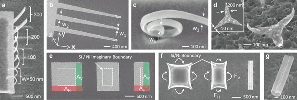 |
| SEM images of the variation of curvature with varying widths showing that nanostructures with both homogeneous and varying radii of curvature can be self-assembled. a) SEM image of the curving of cantilevers with different widths (50, 100, 200, and 300 nm). All cantilevers have the same L=1µm and thickness (Ni 10/Sn 2.5 nm). Cantilevers with the same width show the same radii of curvature, while those of larger widths have larger radii of curvature. This result highlights the reproducibility of the self-assembly process. b) SEM image of cantilevers with varying width along the length of the cantilever (i.e. W1<W2). c) A cantilever with varying width curved with varying radii of curvature due to a varying area moment of inertia, resulting in the formation of a nanospiral. d) Nanoscale three-fingered talon shaped structures before and after coalescence. e,f) Square and rectangular patterns (Sn 5 nm/Ni 5 nm) before and after coalescence developed bending forces FV and FH of different magnitudes and directions. g) Tilted zoomed-in image of the nanoscroll shown in (f). (Reprinted with permission from Wiley-VCH Verlag) |
| In their experiments, the team observed the increase in stress within a tin film deposited on silicon substrate during plasma etching of the substrate, resulting in the edges of the tin film curling up on release from the underlying silicon. |
| "In order to utilize this extrinsic stress to reproducibly curve patterned nanostructures, we investigated the insertion of a continuous film in between the silicon substrate and the tin film to form a multilayer stack" explains Gracias. |
| Various materials such as nickel, alumina or silica could be used for the additional film in the bilayer. Here the team used nickel and alumina. |
| "To retain the induction of grain coalescence observed on bare silicon, it was necessary that the interfacial energy of the additional material was such that the deposited tin film also showed a Volmer?Weber or grain growth, similar to the morphology we observed when tin was deposited on bare silicon," says Gracias. "Then we could induce grain coalescence and the associated extrinsic stress after deposition and during plasma etching of the underlying silicon." |
| The team carried out several control experiments to confirm that the curving of the bilayers was indeed induced by grain coalescence in the tin film. |
| The researchers determined that the etching geometry of the underlying substrate can also be used to control the structure formed. |
| "We observed that square shaped panels curved equally on all four sides, while rectangular shaped panels curved predominantly along the direction of least resistance i.e. along the axis with the smallest area moment of inertia," says Gracias. "Since this assembly process is compatible with conventional e-beam processing, we were able to create curved structures with any desired patterns." |
| To do that, the researchers first defined the desired structures in 2D using e-beam lithography with line widths as small as 20nm. To demonstrate patterning versatility, they defined structures with pores and the letters JHU and NANOJHU on them. When grain coalescence was induced, these structures curved spontaneously to form porous nanotubes and lithographically patterned scrolls, rings, and hooks. |
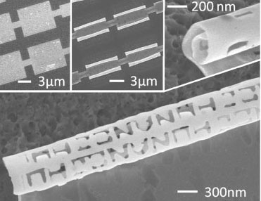 |
| Nanostructures such as rings and scrolls with the letters JHU and NANOJHU patterns on them. (Reprinted with permission from Wiley-VCH Verlag) |
| Gracias notes that at the present time the team is using electron beam lithography to pattern the 2D templates that spontaneously assembled into the 3D structures. |
| "Hence, although the assembly is highly parallel and cost-effective, the 2D patterning is not" he says. "We would like to use other means of patterning to enable mass production of these structures in a parallel and cost-effective manner." |
 By
Michael
Berger
– Michael is author of four books by the Royal Society of Chemistry:
Nano-Society: Pushing the Boundaries of Technology (2009),
Nanotechnology: The Future is Tiny (2016),
Nanoengineering: The Skills and Tools Making Technology Invisible (2019), and
Waste not! How Nanotechnologies Can Increase Efficiencies Throughout Society (2025)
Copyright ©
Nanowerk LLC
By
Michael
Berger
– Michael is author of four books by the Royal Society of Chemistry:
Nano-Society: Pushing the Boundaries of Technology (2009),
Nanotechnology: The Future is Tiny (2016),
Nanoengineering: The Skills and Tools Making Technology Invisible (2019), and
Waste not! How Nanotechnologies Can Increase Efficiencies Throughout Society (2025)
Copyright ©
Nanowerk LLC
|

Become a Spotlight guest author! Join our large and growing group of guest contributors. Have you just published a scientific paper or have other exciting developments to share with the nanotechnology community? Here is how to publish on nanowerk.com. |
