| Posted: Oct 26, 2010 | ||
'Cooking' sharper AFM tips in a microwave oven |
||
| (Nanowerk Spotlight) Atomic force microscopy (AFM) techniques utilize tiny, nanometer-sharp tips to manipulate nanostructures and devices by scanning or rather sliding in very close proximity over the surface – similar to the way the needle of a record player on a record (if you are old enough to remember record players...). These techniques are established tools for scientists to explore the nanocosmos and to achieve the highest possible resolution allowing research on the molecular or even atomic scale. | ||
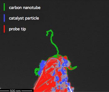
| In atomic force microscopy, tip quality depends mainly on the dimensions and shape of the probe, the durability of the tip apex, and the nature of the interaction between sample and probe. With this in mind, researchers have experimented with mounting ultra sharp and high aspect ratio carbon nanotube (CNT) bundles onto the apex of an AFM tip to improve spatial and potential resolution (see for instance: "High resolution surface potential imaging with ultrasharp carbon nanotubes"). | ||
| Although AFM tips functionalized with a carbon nanotube have attracted considerable attention, attaching CNTs to scanning probes is not a trivial matter (see for instance: "Nanotechnology gets a grip"), which limits their practical use. An alternative approach, whereby a CNT is grown onto the AFM tip (see for instance: "Nanotechnology listening device for neuronal talks"), also can be very time-consuming and requires a costly set-up. | ||
| A team at the Friedrich-Schiller-University Jena in Germany has now demonstrated a fast and cheap process for the fabrication of carbon nanotube AFM tips with the help of microwave ovens. | ||
"Our new technique allows the fabrication of carbon nanotube AFM probes utilizing the microwave-assisted growth of CNTs directly on the apex of a commercially available AFM tip" Tamara Druzhinina, PhD student in the group, tells Nanowerk.
Stephanie Höppener, heading the 'Nanolithography and Surface Functionalization' group in Ulrich S. Schubert's laboratory at Jena points out that the technical requirements are relatively low compared to other approaches (no furnace is needed) and it is safe to work with just a little amount of liquid ethanol (no acetylene, no hydrogen is required). The team reported their findings in a recent issue of Nano Letters "Microwave-Assisted Fabrication of Carbon Nanotube AFM Tips"). Previously, the team had observed that in particular on the edges of silicon wafers treated in a normal kitchen microwave, melting of the silicon wafer can occur. Considering the high temperatures which are required to melt silicon, they concluded that potentially suitable conditions for the growth of CNTs could be generated as well (see: "The Selective Heating of Iron Nanoparticles in a Single-Mode Microwave for the Patterned Growths of Carbon Nanofibers and Nanotubes"). |
||
| By experimenting with different amounts of catalyst material, the researchers managed to optimize the the catalyst deposition process to ultimately be able to grow individual CNTs on an AFM tip. | ||
Due to its relative simplicity, a microwave-assisted approach could lead to much cheaper CNT-functionalized scanning probe tips. Today, high resolution probes for Scanning Force Microscopy can easily cost 350 euros or more. "With our process we can reach a price level that would justify the use of such tips also just for routine measurements," says Höppener. One challenge that the team is working on is controlling the growth direction of the CNTs. Whereas that issue has been solved in bulk and microstructured films, it still poses a problem for single carbon nanotubes on AFM tips. |
||
 By
Michael
Berger
– Michael is author of four books by the Royal Society of Chemistry:
Nano-Society: Pushing the Boundaries of Technology (2009),
Nanotechnology: The Future is Tiny (2016),
Nanoengineering: The Skills and Tools Making Technology Invisible (2019), and
Waste not! How Nanotechnologies Can Increase Efficiencies Throughout Society (2025)
Copyright ©
Nanowerk LLC
By
Michael
Berger
– Michael is author of four books by the Royal Society of Chemistry:
Nano-Society: Pushing the Boundaries of Technology (2009),
Nanotechnology: The Future is Tiny (2016),
Nanoengineering: The Skills and Tools Making Technology Invisible (2019), and
Waste not! How Nanotechnologies Can Increase Efficiencies Throughout Society (2025)
Copyright ©
Nanowerk LLC
|
||

Become a Spotlight guest author! Join our large and growing group of guest contributors. Have you just published a scientific paper or have other exciting developments to share with the nanotechnology community? Here is how to publish on nanowerk.com. |