| Posted: Mar 06, 2014 |
AFM and Raman spectroscopy-correlated imaging and tip enhanced Raman scattering |
| (Nanowerk Application Note) The desire to identify materials and their properties to understand complex systems and better engineer their functions has been driving scanning probe microscopies since their inception (see figure 1). Both atomic force microscopy (AFM) and Raman spectroscopy are techniques used to gather information about the surface properties and chemical information of a sample. There are many reasons to combine these two technologies, and this application note discusses both the complementary information gained from the techniques and how a researcher having access to a combined system can benefit from the additional information available. |
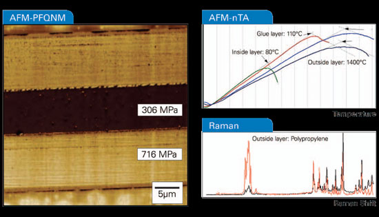 |
| Figure 1. Atomic force microscopy and correlated optical spectroscopies can yield information about the sample composition (here a cross section of some food packaging material), shape, and various other properties, such as nanomechanical maps and thermal property maps. |
| Two Surface Analysis Methods |
| Atomic force microscopy — In atomic force microscopy, a sharp tip is brought into close proximity with a sample and held at that distance by means of a force-based feedback loop.1 In addition to the force on which the primary feedback loop is based, different quantities such as electrical current, surface potential, or specific nanomechanical properties can be measured. By scanning tip and sample relative to each other and measuring these quantities at discrete locations in a serial fashion, three-dimensional images of selected sample properties can be created. The information from atomic force microscopy has proven to be extremely useful for scientific research, but it lacks the chemical specificity available from vibrational spectroscopies. |
| Raman spectroscopy — Spectroscopy is the study of the interaction of electromagnetic radiation with matter. The most common kinds are X-ray, fluorescence, infrared, and Raman.2 The latter two are vibrational techniques, i.e., the energy of radiation employed is sufficient to excite molecular or lattice vibrations. In a Raman experiment the sample is illuminated with monochromatic light, and the inelastically scattered light is detected. If a sample is illuminated with light of a frequency √0, most of the scattered light is Raleigh scattered, i.e., elastically scattered without a change in frequency. A small portion, however, is scattered at a different frequency √1 because of a change in the polarizability of the illuminated molecule. This shift is referred to as the Stokes shift if √1 is red-shifted with regard to the incident light, or anti-Stokes if √1 is blueshifted. |
| A plot of the measured intensity of these shifts versus the frequency is referred to as a Raman spectrum and is a representation of the vibrational modes of the molecules or solids to be investigated or indentified. |
| Raman spectroscopy can provide information about a variety of materials-related phenomena: (a) molecular composition by analyzing bands at characteristic frequencies (fingerprint); (b) symmetry or orientation of molecules or crystals by monitoring peaks using polarization selection for the incident and scattered light;4 or (c) measurement of stress or strain in a crystal by analyzing e.g., the frequency shift of a characteristic Raman band. (See reference 5 for an in-depth review article on how Raman spectroscopy can be applied to popular carbon allotropes.) |
| As a direct probe of the vibrational structure, Raman does not depend on the presence of a chemically less specific electronic state with high fluorescence quantum yield, giving it wide applicability as a specific probe of chemical composition and symmetry. This can be especially useful for the analysis of bio-materials since Raman, unlike fluorescence, does not require labeling of the sample. |
| What makes Raman spectroscopy challenging is that its cross section is quite small. Only one in a million photons interacting with a sample will be inelastically scattered and thus exhibit a Raman shift, while the other photons are simply Raleigh scattered. In order to get enough signal for analysis, acquisition times of several tens of seconds per location may become necessary. |
| Raman microscope — A Raman spectrometer is often combined with an optical microscope to take advantage of the high spatial resolution that a confocal optical setup can offer. The main components of a dispersive Raman setup are a continuous wave laser to illuminate the sample, high NA optics to collect the backscattered radiation, a laserline rejection filter, and a spectrometer consisting of an entrance slit, a diffraction grating, and a CCD camera. |
| Analytical spatial resolution is limited by diffraction and for a conventional upright Raman setup is typically 500nm to 1µm with a depth of focus of around 1µm. As an example, the lateral resolution in a transmission mode setup, with an oil-objective NA of 1.2 and red laser light, may be calculated to be 322nm, using the Raleigh criterion: |
| R = 0.61 • λ/NA |
| Bringing AFM and Raman spectroscopy together offers a way to improve this spatial resolution of analysis. |
| Combining AFM with Raman Spectroscopy |
| Tip Enhanced Raman Scattering (TERS) — The full synergistic effect of AFM and optical spectroscopies comes into play when the AFM tip is tasked with “becoming the light source.” With the end radius of an AFM tip <20nm, i.e., much smaller than the conventional diffraction limit spot size, 30-50 times higher spatial resolution can be obtained. In near-field microscopy, one uses the effect that a small object brought into a propagative field induces an evanescent wave and vice versa. One of the characteristics of evanescent waves is that they decay exponentially with increasing distance, which offers a gateway to resolution beyond the classical diffraction-based limitations. This requires the light source and sample to be at a distance from each other that is much smaller than the wavelength of light used, i.e., the optical near-field.6 |
| By using a suitable AFM tip as a scatter light source and subsequently scanning the sample, tip-assisted optical spectroscopy measurements can be performed (see figure 2). |
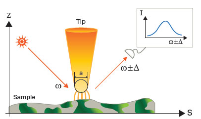 |
| Figure 2. General setup for linear and non-linear tip-assisted Scanning Probe Microscopy (SPM) and optical spectroscopies. A sharp tip is brought into the optical near-field and illuminated from the side. The backscattered light from the tip-sample gap is detected in the far-field using a suitable detection scheme. For TERS the tip has to be metallized so that the surface plasmon can be excited, which will then give rise to the typically seen enhancement factors. |
| Continue to next page (2 of 4) |
|
|

Become a Spotlight guest author! Join our large and growing group of guest contributors. Have you just published a scientific paper or have other exciting developments to share with the nanotechnology community? Here is how to publish on nanowerk.com. |
