| Posted: Jul 29, 2014 |
Printed paper memory |
| (Nanowerk Spotlight) It seems that computer memory technology is coming full circle. Pioneers in the early 19th century, such as Charles Babbage, first proposed the use of paper memory (albeit non-electronic), where a bit was stored as the presence or absence of a hole in a paper card. State-of-the-art research today again is proposing the use of paper as memory devices. This time, although he paper may be very similar, the bits are not crudely punched holes but nanofabricated device structures. |
| Traditionally, electronic devices are mainly manufactured by photolithography, vacuum deposition, and electroless plating processes. In contrast to these multi-staged, expensive, and wasteful methods, inkjet printing offers a rapid and cheap way of printing electrical circuits with commodity inkjet printers and off-the-shelf materials (Read more: "Conductive nanomaterials for printed electronics applications"). |
| Although transparent plastic substrates are widely explored for flexible electronics (read more: "The rise of flexible electronics"), they have intrinsic problems: Most of them are not thermally stable; are not based on green – i.e. renewable and biodegradable – materials; and are not as easily printable as paper. |
| Recently, researchers have explored papers with the goal of replacing plastic substrates as a lightweight substrate for low-cost, versatile, and roll-to-roll printed electronics. Already, they have demonstrated various types of devices on papers such as batteries ("Truly green paper battery is algae-powered"), solar cells ("Mass-printed polymer/fullerene solar cells on paper"), or RFID tags ("Playing RFID tag with sheets of paper"), and even transistors ("Nanopaper transistors for the coming age of flexible and transparent electronics"). |
| In new work, researchers from National Taiwan University demonstrated a paper-based, nonvolatile memory device. As they reported in the July 14, 2014 online edition of ACS Nano ("All-Printed Paper Memory"), the team used a combination of inkjet and screen printing to fabricate resistive RAM memory cells on commercial printing paper. |
| Electronics printed on paper are cheap, flexible, and recyclable, and could lead to applications such as smart labels on foods and pharmaceuticals or as wearable medical sensors. |
| This is the first nonvolatile memory built on paper. Resistive random access memory (RRAM), however, is not a new concept. The combination of RRAM and paper is ideal because the structure of RRAM is simple—only one insulator and two electrodes are required for a bit. Operation is also simple; such memory is operated by changing the resistances of the insulator material, whose resistive states – 0 and 1 – varies greatly as different voltages impose across it. In addition, RRAM is nonvolatile so an embedded power source is not required. |
| "One challenge of using regular cellulose paper as a base for electronic memory is that, because it is made of fibers, it is very rough and porous on a microscopic level, making it difficult to lay down the thin, uniform layers of materials that typical memory technologies require," Jr-Hau He, an Associate Professor at the Institute of Photonics and Optoelectronics & Department of Electrical Engineering, National Taiwan University, who led the work, explains to Nanowerk. |
| To get around this problem, He's team decided to fabricate RRAM, a relatively new type of memory with a structure simple enough to cope with such surface variations. |
| In an RRAM device, an insulator can be set to different levels of electrical resistance by applying a voltage across it; one level of resistance corresponds to the 1s of digital logic, the other to the 0s. So each bit in RRAM consists of an insulator sandwiched by two electrodes. |
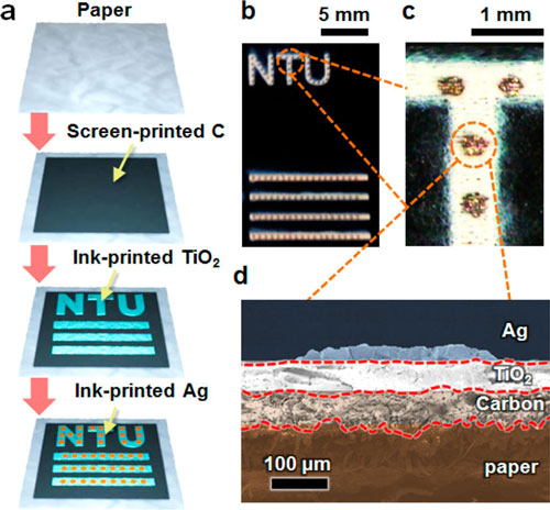 |
| Fabrication and geometry of a paper RRAM. (a) Schematic diagram of the fabrication process for the resistive paper memory device. (b) Photograph of the device taken by optical microscopy. The alphabetical letters and the line arrays composed of Ag and TiO2 demonstrate the degree of freedom for the inkjet-printed patterns. (c) Zoom-in optical image from b. (d) Cross-sectional scanning electron microscopy image of the paper-based memory. (Reprinted with permission by American Chemical Society) |
| This device is fabricated by printing techniques – inkjet printing and screen printing – so the memory can be printed by a commercial printer or roll-to-roll techniques. In a first fabrication step, commercial printing paper is coated several times – until the surface roughness of the paper is smoothed out – with a layer of carbon paste that will serve as the bottom electrode. After curing, patterns of titanium oxide nanoparticles are inkjet-printed onto the paper and dried. Finally, silver nanoparticle ink is inkjet-printed on top of the TiO2 patterns in order to form the top electrode. |
| He notes that, if combined with other printable devices, it will become possible for consumers to design a functional circuit on their own computer, or download one from the internet, and directly fabricate it at home instead of in a lab or factory setting. |
| "And then a lot of applications will become possible," says He. "For example, integrated with RFIDs, a printed RRAM device can be used for ticketing; dot arrays can serve as QR code and provide better security; or it can just be memories embedded in your books, paper cups, or any other printable objects". |
| Going forward, one of the issues the researchers will focus on is to increase the memory density of their printed RRAM. The current work uses a regular inkjet printer and has a dot size of ∼50 µm with pitch resolution of 25 µm. Thus, one bit will occupy a square of about 100 µm on each side, or 104 bits per cm2. With this density, a fully printed A4 paper can hold 6.237*106 bits or roughly 780 KB of data. |
| With a higher resolution printer it will be possible to achieve a dot resolution of 1 µm and nearly the same pitch width. That means the density could be enhanced by about 2500 times, and 1.56*1010 bits, or almost 2 GB, could be obtained on a single A4 paper. |
| According to He, the team is currently exploring RRAM crossbar architectures and trying to build 1D-1R or 2D-1R structures. The cross-bar architecture is possible to be stacked, so that the 3D arrays can be achieved, and the density can be increased. |
| They are also exploring the use of arrays of single memory dots, for instance in arrangements like QR codes. "The dots can be painted, so combining the pigments (dark and light) and resistive states (high and low) the stored information can be doubled and secured," says He. |
 By
Michael
Berger
– Michael is author of four books by the Royal Society of Chemistry:
Nano-Society: Pushing the Boundaries of Technology (2009),
Nanotechnology: The Future is Tiny (2016),
Nanoengineering: The Skills and Tools Making Technology Invisible (2019), and
Waste not! How Nanotechnologies Can Increase Efficiencies Throughout Society (2025)
Copyright ©
Nanowerk LLC
By
Michael
Berger
– Michael is author of four books by the Royal Society of Chemistry:
Nano-Society: Pushing the Boundaries of Technology (2009),
Nanotechnology: The Future is Tiny (2016),
Nanoengineering: The Skills and Tools Making Technology Invisible (2019), and
Waste not! How Nanotechnologies Can Increase Efficiencies Throughout Society (2025)
Copyright ©
Nanowerk LLC
|

Become a Spotlight guest author! Join our large and growing group of guest contributors. Have you just published a scientific paper or have other exciting developments to share with the nanotechnology community? Here is how to publish on nanowerk.com. |
