| Posted: Sep 30, 2015 | |
Measuring femtoscale displacement for photoacoustic spectroscopy |
|
| (Nanowerk Spotlight) The development of nanoscale devices and applications requires ultra-sensitive sensing systems that can offer not only atomic resolution imaging but also sub nanometer scale displacement detection, zeptogram level mass sensing, or single bio-molecular sensing. | |
| Optical scanning methods – the optical transduction of a micro- or nanocantilever's motion – are widely used to achieve high deflection sensitivity down into the sub-nanometer range. | |
| Researchers have now developed a novel sensor that addresses some of the shortcomings that have plagued existing optical scanning systems , namely size, complexity, and cost. They reported their findings in Nature Communications ("Piezotransistive transduction of femtoscale displacement for photoacoustic spectroscopy"). | |
| "Our sensing technology is completely electrical and capable of sensing very small displacement as low as in the femtometer range," Abdul Talukdar, former PhD student from the University of South Carolina-Columbia (currently at Intel Corporation) and the paper's first author, tells Nanowerk. "This sensitivity has enabled the detection of nanogram level explosives (RDX) and other analytes." | |
| The research team, which included scientists from the universities of South Carolina, Alberta, Calgary, and Clemson University, Talukdar and principal investigator Prof. Goutam Koley developed on III-V nitride based microcantilever embedded with a highly sensitive three-terminal device or heterojunction field effect transistor (HFET). | |
 |
|
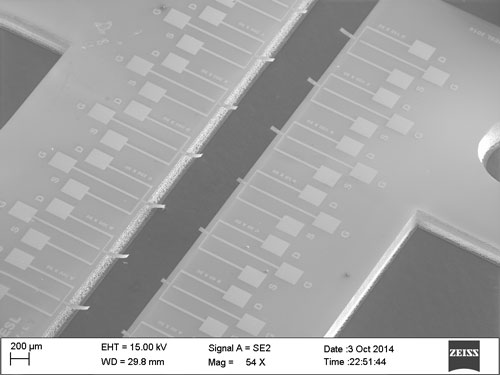
| SEM image of AlGaN/GaN HFET embedded GaN Microcantilevers array (14 microcantilevers) for the integration of different sensing attributes. (Image: Abdul Talukdar) (click on image to enlarge) | |
| With the collaboration from Canada, the research team has demonstrated for the first time, real-time sensing of nanogram level explosive material has been done photoacoustically and with a completely electrical readout. | |
| The researchers found that, utilizing the piezoelectric properties of III-V nitride materials, the piezoelectric polarization-induced changes in two-dimensional electron gas can be utilized to transduce displacement with very high sensitivity. | |
| "Thus it is possible to detect femtoscale displacement with a microcantilever operating below 100 kHz without moving towards a nanocantilever operating at MHz, which is very difficult to fabricate thus offer low yield, require complex measurement systems, and often very costly," says Talukdar. | |
| He adds that, while current research trends in cantilever-based sensing appears to be moving toward nanoscale devices, this involves complex fabrication schemes that sometimes are hard to replicate and to confirm their comparable performance. | |
| By utilizing inherent piezoelectric material properties and a heterojunction transistor embedded at the base of a microcantilever – what the team calls a 'piezotransistive microcantilever' – the device offers very high sensitivity with a very simple measurement technique. | |
| The demonstrated sensitivity of this device is the best among the state-of-the-art electrical technologies, notes Talukdar. | |
| The results published in the paper show electrical sensing performance comparable to optical means, and thus advancing the possibility of replacing optical readouts with electrical readouts from relevant equipment to offer cheaper, lighter, smaller, and better devices. | |
| Importantly, the new device can readily be implemented in any scanning probe based microscopy – such as Atomic Force Microscopes – eliminating the need for optical readout; it can can be used as array based sensing in real time; as strain, force, and displacement sensor. | |
| The team points out that, as the materials (AlGaN/GaN) are optically transparent, they can easily be integrated with wearable technologies for instance for health monitoring. | |
| Aluminum nitride and gallium nitride, two materials with wide bandgap strong piezoelectric properties, are also often used in devices that need to operate in harsh environments. Therefore these new sensors lend themselves to space and aircraft applications, and any other mission in remote areas under extreme pressure and temperature. | |
| The next stage of this work is to integrate the complete sensing system into a single portable package. Another goal is to demonstrate array-based sensing and imaging to detect multiple analytes (e.g. different explosives) in real time. | |
| Talukdar cautions that there are two key challenges for this novel senor technology: | |
| Firstly, AlGaN/GaN is less defective when grown on SiC or Sapphire. But for cantilever based MEMS/NEMS, a silicon substrate is desirable. However AlGaN/GaN on Si is more defective. Thus the challenge is defect-less material growth on Si, a task which already has progressed significantly. | |
| Another major challenge for this technology, when used in photoacoustic spectroscopy, is the generation of acoustic waves from an analyte which eventually oscillate the microcantilever and the HFET detects the deflections. | |
| "A laser system/light source is needed to excite the analytes with sufficient power, however these laser systems are bulky, costly, and power hungry," Talukdar explains. "Thus, even with replacing the optical readout with the piezotransistor, which significantly reduces the size, cost, and the power consumption, it still is the excitation laser source that hinders further miniaturization and simplification. Only with a better excitation source can the whole system be packaged into a hand-held portable spectroscopy system." | |
 By
Michael
Berger
– Michael is author of three books by the Royal Society of Chemistry:
Nano-Society: Pushing the Boundaries of Technology,
Nanotechnology: The Future is Tiny, and
Nanoengineering: The Skills and Tools Making Technology Invisible
Copyright ©
Nanowerk LLC
|
|
|
Become a Spotlight guest author! Join our large and growing group of guest contributors. Have you just published a scientific paper or have other exciting developments to share with the nanotechnology community? Here is how to publish on nanowerk.com. |
|
