| May 31, 2019 |
Let's do the twist - rotation-tunable 2D electronics |
| (Nanowerk Spotlight) Ever since the isolation of graphene in 2004, the rapidly growing family of two-dimensional (2D) materials (more than 2,500 other layered, atomically thin, materials have been identified so far) cover an amazing range of electrical, chemical, optical and mechanical properties. |
| Perhaps the most astounding discovery is that they can be combined freely to create altogether new materials, so called van der Waals heterostructures. By stacking together any number of atomically thin layers, it becomes possible to create novel metamaterials and devices otherwise not achievable by traditional three-dimensional materials. |
| Researchers commonly observe a relative rotation between individual layers of 2D materials. Importantly, these interlayer rotation angles, i.e. at what angle two individual layers are oriented towards each other, influence the electronic properties of the resulting material system. |
| Scientists have not yet been able to explain why, during CVD growth of 2D layers, there is such a wide range of rotation angles of nucleated domains, leading to significant grain boundary formation. |
| However, control over the rotation of the constituent 2D flakes is required in order to precisely tailor a material's electronic properties. This rotation-tunable design parameter is at the core of the emerging field of nanoscale twistronics. |
| Reporting their findings in ACS Nano ("Controlling Rotation of Two-Dimensional Material Flakes"), researchers reveal a general moiré-driven mechanism that governs the interlayer rotation. |
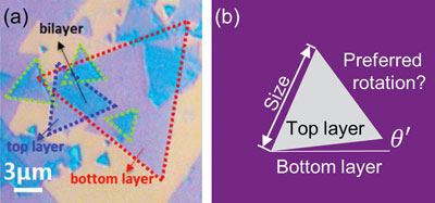 |
| (a) Triangle-shaped nucleated domains of MoS2 bilayers grown by CVD. Many interlayer rotation angles can be observed (This imaged is adapted with permission from Nano Lett. 2014, 14, 5500-5508. Copyright 2014 American Chemical Society). (b) In a 2D bilayer system, how does the preferred rotational orientation relate to the flake size? (Reprinted with permission by American Chemical Society) |
| "We have discovered that for a small flake of crystalline material that is weakly bonded to a crystalline substrate, it is possible to induce rotation of the flake by applying strain to the substrate," Harley T. Johnson, a professor at the University of Illinois at Urbana-Champaign, tells Nanowerk. "At the core of our findings is the concept of the van der Waals dislocation, which is the term we use to describe the commensurability/incommensurability defect in bilayer crystalline materials." |
| Johnson and his collaborators have described this concept in a recent paper in Applied Materials Today ("Toward Moiré engineering in 2D materials via dislocation theory") |
| "Realizing that relative strain and rotation between a crystalline bilayer can be understood in terms of moiré patterns, which consist of van der Waals dislocations, it gives us a clear way to explain the energetics that control rotation of 2D material flakes," he adds. "We are starting to understand the mechanics of these weakly interacting bilayer systems in new ways, and as we do, we realize that many of the interesting experimental observations that have been made in the past few years can be explained using the new framework that we are have developed." |
| The fact that moiré patterns are dislocations implies that the energetics of the dislocations will have interesting consequences for certain material systems at certain length scales – and researchers are seeing those implications in nanoscale 2D material systems. |
| As a result of this new understanding it will become possible for materials scientists to 'dial in' the desired rotation between 2D layers by applying the appropriate amount of strain to the substrate. |
| For example, this new observation may make it possible to achieve the particular relative rotation between flake and substrate required for the recently discovered 'magic' angle effect in bilayer graphene, at which unconventional superconductivity can be found. |
| The next stage for Johnson's team is to explore the precise strain-rotation relationships for a variety of materials and flake sizes, so that one can use the observation for rational design of next generation microelectronic and optoelectronic devices. |
| "We are continuing to explore the implications of the delicate energy balance associated with commensurability and incommensurability in 2D material systems, and the possible effects this energy balance will have for electronic properties of devices," he concludes. "Obviously there are challenges in achieving synthesis and fabrication of device geometries, and in working with certain 2D materials, but the variety of materials that are now available is also tremendously interesting – this is the promise of van der Waals heterostructures." |
 By
Michael
Berger
– Michael is author of four books by the Royal Society of Chemistry:
Nano-Society: Pushing the Boundaries of Technology (2009),
Nanotechnology: The Future is Tiny (2016),
Nanoengineering: The Skills and Tools Making Technology Invisible (2019), and
Waste not! How Nanotechnologies Can Increase Efficiencies Throughout Society (2025)
Copyright ©
Nanowerk LLC
By
Michael
Berger
– Michael is author of four books by the Royal Society of Chemistry:
Nano-Society: Pushing the Boundaries of Technology (2009),
Nanotechnology: The Future is Tiny (2016),
Nanoengineering: The Skills and Tools Making Technology Invisible (2019), and
Waste not! How Nanotechnologies Can Increase Efficiencies Throughout Society (2025)
Copyright ©
Nanowerk LLC
|

Become a Spotlight guest author! Join our large and growing group of guest contributors. Have you just published a scientific paper or have other exciting developments to share with the nanotechnology community? Here is how to publish on nanowerk.com. |
