| Mar 02, 2021 |
Rolling 2D van der Waals heterostructures into 1D nanotubes |
| (Nanowerk Spotlight) Ever since the first demonstration of graphene in 2004, scientists have discovered more than 2 500 other layered, atomically thin (two-dimensional, 2D), materials. While these materials cover an amazing range of electrical, chemical, optical and mechanical properties, perhaps the most astounding discovery is that these crystals can be combined freely to create altogether new materials: When two or more 2D materials are placed on top of each other their properties change, and a material with novel hybrid properties emerges. |
| While strong covalent bonds provide in-plane stability of the 2D crystals, these materials are called van der Waals heterostructures because the atomically thin layers are not mixed through a chemical reaction but rather attached to each other via a weak, so-called van der Waals interaction – similar to how a sticky tape attaches to a flat surface. |
| The properties of these hybrid material can be precisely controlled by twisting the stacked atomic layers, opening the way for the use of this unique degree of freedom for the nanoscale control of composite materials and nano-devices in future technologies. |
| Of course, the research community didn't stop there. Intrigued by the possibilities offered by 2D van der Waals heterostructures, the exploration of one-dimensional (1D) analogs of these heterostructures began. |
| Just recently, researchers at the Maruyama-Chiashi laboratory at the University of Tokyo have succeeded by basically rolling a stacked 2D heterostructure into a thin (5nm diameter) cylinder (Science, "One-dimensional van der Waals heterostructures"). |
| This work suggests that all 2D materials could also be rolled into their 1D counterparts and a plethora of function-designable 1D heterostructures could be realized. Unlike semiconductor nanowires or mono-elemental nanotubes, which are rolls of one type of material, these novel nanostructures would have very different, and customizable, properties. |
| The invention of heteronanotubes by Prof. Maruyama's team opens a new class of materials that could become a new platform for many types of devices. |
| The UTokyo team, together with Prof. Slava V. Rotkin's team at Penn State, now went one step further by demonstrating, for the first time, the operation of a 1D diode made of a 1D van der Waals heterostructure. |
| Reporting their findings in ACS Nano ("One-Dimensional van der Waals Heterojunction Diode"), the team demonstrates a 1D heterostructure nanotube with the coaxial assembly of a semiconducting single-walled carbon nanotube, insulating boron nitride nanotube, and semiconducting molybdenum disulfide nanotube, which induces a radial semiconductor-insulator-semiconductor heterojunction. |
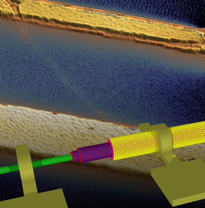 |
| A cartoon of the diode device structure with metal electrodes over the heterotube. The background is a real sSNOM map of the device at one excitation laser frequency, where the hBN shell of the heterotube brightly reflects the light. The size of the image is about 4x6 micrometers. The diameter of the entire roll is about ∼20 nm (including outer MoS2 semiconductor shells, middle hBN insulator shells, and inner carbon/graphene conductor shell). (Image: Prof. Xiang, UTokyo, Prof. Rotkin, Penn State) |
| "This heterotube is an 'old brother' of a nanotube and a 'cousin' of 2D materials, however it is very different from what material scientists produced in the past," says Rotkin. "We showed that it can work as an extremely small diode with high performance despite its small size. |
| Most optoelectronics devices – photodetectors, solar cells, light emitting devices, etc. – are diodes. While a single diode is a signal rectifier, two diodes, connected back-to-back, may also serve as an electronic switch (i.e. transistor). These 1D diodes could offer an alternative method to further miniaturizing optoelectronic building blocks. |
| Rotkin's contribution to this research was to solve a very challenging task: how can you know for sure that this heterostructure cylinder is made with all layers required for a specific one-dimensional van der Waals heterostructure. |
| "To use a sandwich-roll terminology: How do you know whether you have tuna along the whole length of a roll or whether there are empty regions where we have only rice and cucumber," says Rotkin. "Because if that were the case it would mean we did not succeed in making the right heterostructure." |
| In flat van der Waals heterostructures this verification can be done quite easily because it is possible to collect a lot of signals from large flat areas, i.e., the components are very well visible. When you roll these heterostructures up, they become very thin cylinders where the inner sheets become practically invisible and hard to characterize. |
| "In addition, we had have to resolve not only the outer shell of the heterotube, but the middle one," Rotkin points out. "The hBN is an insulator layer between the carbon (inner) and MoS2 semiconductor (outer). Absence of the right insulator between metal and semiconductor would create a short in the diode structure." |
| Scattering Scanning Near-field Optical Microscopy (sSNOM) is ideally suited to perform such a challenging measurement: it can 'see' objects of nanoscale size and determine their materials' optical properties. |
| In order to obtain the record resolution shown in the figure above, Rotkin developed a special method of acquisition and analysis of the sSNOM data: hyperspectral optical imaging with nanometer resolution. |
| The image below shows how the hBN shell lights up in the spectral region of intrinsic vibrations of the hBN material. Using this spectral signature, researchers can do 'structure-testing' of the 1D-diode along its entire length and tell if the insulating material is there. |
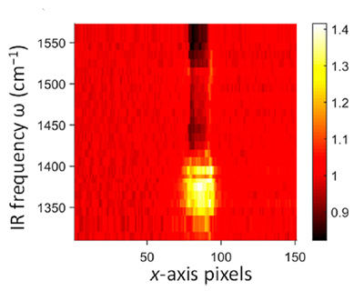 |
| s-SNOM hyperspectral cross section: profiles taken of the heterotube and normalized to the background, from scans at IR frequencies of 1310∼1573 cm-1. (Reprinted with permission from American Chemical Society) |
| "As far as I know this is the first demonstration of the optical resolution of a hexagonal boron nitride (hBN) shell as a part of a hetero-nanotube," Rotkin notes. "Much larger multiwall mono-elemental hBN nanotubes (many shells of hBN) as well as carbon nanotubes were studied in the past, with similar microscopes. However, imaging these tubes is quite different from what we have done; it perhaps is comparable to the difference between seeing a wood log and seeing a graphite rod inside a pencil – through the pencil walls." |
| Rotkin and his collaborators are currently working to expand these studies in terms of both theoretical and experimental aspects of sSNOM imaging for various nanomaterials – from glass (see Acta Materialia "Subsurface structural change of silica upon nanoscale physical contact: Chemical plasticity beyond topographic elasticity") to 2D materials (work in progress) to protein tubules and viruses. |
| It is a novel technique where, hopefully, future discoveries should happen. As Rotkin put it: "To me, the fact that we could get optical spectral images from such a small object as a single shell of a heterotube is amazing. As it was emphasized many times, we have two infinities in our Universe – one at far galaxies, another one at the atomic level. Being able to get this image of the hBN shell of a heteronanotube to me is akin to finding exoplanets in far space." |
 By
Michael
Berger
– Michael is author of four books by the Royal Society of Chemistry:
Nano-Society: Pushing the Boundaries of Technology (2009),
Nanotechnology: The Future is Tiny (2016),
Nanoengineering: The Skills and Tools Making Technology Invisible (2019), and
Waste not! How Nanotechnologies Can Increase Efficiencies Throughout Society (2025)
Copyright ©
Nanowerk LLC
By
Michael
Berger
– Michael is author of four books by the Royal Society of Chemistry:
Nano-Society: Pushing the Boundaries of Technology (2009),
Nanotechnology: The Future is Tiny (2016),
Nanoengineering: The Skills and Tools Making Technology Invisible (2019), and
Waste not! How Nanotechnologies Can Increase Efficiencies Throughout Society (2025)
Copyright ©
Nanowerk LLC
|

Become a Spotlight guest author! Join our large and growing group of guest contributors. Have you just published a scientific paper or have other exciting developments to share with the nanotechnology community? Here is how to publish on nanowerk.com. |
