| Jun 17, 2021 |
Structural engineering on the atomic scale |
| (Nanowerk Spotlight) The arrangement of the constituent atoms in a solid material's crystal structure determines its properties. Technologies such as electron and x-ray crystallography can reveal the atomic geometry of a crystal – however, they do not identify the precise location and position of each individual atom. |
| But when the dimensions of a material shrink to the nanoscale, the location and position of each individual atom becomes critically important. |
| Case in point is graphene, which is especially sensitive to defects in its atomic structure. One of the keys to exploiting graphene's enormous potential is the ability to create atomic-scale defects – where carbon atoms in its flat, honeycomb-like structure are rearranged or 'knocked out' – as these influence its electrical, chemical, magnetic, and mechanical properties. |
| For the enormous promises of graphene and other two-dimensional (2D) materials to be fulfilled, however, scientists need a much better understanding of how specific types of defects in the crystal structure, including those that change location over time, affect its properties. To do that, they first need to identify the location and type of defect and then be able to precisely alter the structure of 2D materials in order to tailor their properties for applications based on them. |
| "Until now, microscopic characterization of defect-engineered materials has been limited to a handful of images due to challenges in large-scale characterization," Alberto Trentino, a PhD candidate in the Physics of Nanostructured Materials group at the University of Vienna, tells Nanowerk. "Because of this, the results of defect-engineering have been only quantified indirectly via spectroscopic techniques." |
| Trentino is first author of a paper in Nano Letters ("Atomic-Level Structural Engineering of Graphene on a Mesoscopic Scale") that demonstrates structural engineering and atomic-scale analysis of graphene up to a level that so far has not been possible. |
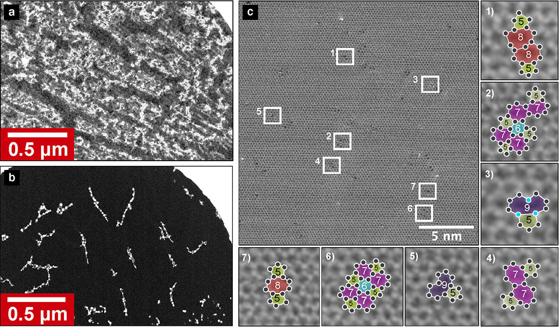 |
| Atomic structure before and after cleaning and ion irradiation. (a) STEM-ADF images of suspended graphene before and after (b) laser cleaning in the microscope column. The entire dark area in (b) corresponds to atomically clean graphene. (c) An example STEM-ADF image of a sample area with a particularly high defect density after Ar+ irradiation, demonstrating that even defected areas have remained contamination free during the process. Seven of the defects are further shown at higher magnification to demonstrate the variety of different defect types that can be created during the irradiation process. They include monovacancies V1(59) (c.3, c.5), a trivacancy V3(5885) (c.1), divacancies V2(55−8) (c.7) and V2(55−77) (c.4), and more complex structures (c.2 and c.6). The light blue dots in c.3 mark possible impurity atoms based on the image contrast. (Reprinted with permission by American Chemical Society) (click on image to enlarge) |
| With the results from this work, spectroscopic fingerprints can for the first time be directly compared to the atomic structure of the sample. This will allow checking whether the models that have been used until now to explain those fingerprints are indeed correct. |
| This work also takes the first important step towards automated acquisition of atomic resolution images of 2D materials, opening scanning transmission electron microscopy to large-scale material characterization also for disordered or defected structures. |
| Additionally, as Trentino points out, the team's experimental setup comprising a laser and a plasma ion source in the same connected vacuum setup with the electron microscope demonstrates the importance of protecting defect-engineered samples from ambient conditions between characterization and manipulation. |
| Completing this setup of an ultrahigh vacuum system combined with automated image acquisition is a convolutional neural network trained to reliably recognize atomic structure from microscopy images to deduce the topology of defected areas. |
| The team carried out, for the first time, atomic-scale analysis of defected structures at the micrometer scale by automatic imaging and machine-learning-based analysis techniques developed by them. As a result, they can compose a complete picture of the sample by putting together our images like pieces of a puzzle. |
| "We chose graphene as our example material due to the general interest in tailoring its properties through structural engineering and because defected graphene has a very prominent Raman spectroscopy fingerprint that allows a direct comparison of the fully characterized structurally engineered structure to earlier research relying on this fingerprint," says Trentino. "However, none of the three methods we demonstrated here is limited to graphene and could equally well be applied to any sample suitable for transmission electron microscopy characterization." |
| Together, the methods demonstrated in this work show that graphene can be cleaned on a large scale using laser irradiation in vacuum; it can be defect-engineered with plasma ion irradiation that creates only specific types of vacancy-type defects; and that even defective or disordered materials can be characterized at the atomic level using automation and machine learning techniques. |
| "Since we now know the exact atomic structure of the modified material, our results allow correlating it with macroscopic material properties and spectroscopic signatures," Trentino notes. "At the same time, the results establish large-scale defect-engineering as a promising technique to shape graphene, and other 2D materials, for future technologies." |
| In further developing their atomic-level structural engineering of 2D materials, the team now plans to use the created defects in graphene as anchoring sites for impurity atoms. This may allow applications in catalysis and optoelectronics, depending on the atomic species used. They can also serve as nucleation sites for growing completely new materials using graphene as the substrate. |
| "We are very excited to see what will be possible now that our study has been published, and the scientists around the world have access to the same methods," Trentino concludes. "The biggest limitation will be our collective imagination." |
 By
Michael
Berger
– Michael is author of four books by the Royal Society of Chemistry:
Nano-Society: Pushing the Boundaries of Technology (2009),
Nanotechnology: The Future is Tiny (2016),
Nanoengineering: The Skills and Tools Making Technology Invisible (2019), and
Waste not! How Nanotechnologies Can Increase Efficiencies Throughout Society (2025)
Copyright ©
Nanowerk LLC
By
Michael
Berger
– Michael is author of four books by the Royal Society of Chemistry:
Nano-Society: Pushing the Boundaries of Technology (2009),
Nanotechnology: The Future is Tiny (2016),
Nanoengineering: The Skills and Tools Making Technology Invisible (2019), and
Waste not! How Nanotechnologies Can Increase Efficiencies Throughout Society (2025)
Copyright ©
Nanowerk LLC
|

Become a Spotlight guest author! Join our large and growing group of guest contributors. Have you just published a scientific paper or have other exciting developments to share with the nanotechnology community? Here is how to publish on nanowerk.com. |
