| May 05, 2022 |
Synthesis, properties and applications of 2D materials beyond graphene |
| (Nanowerk Spotlight) In two-dimensional (2D) nanomaterials, two dimensions are outside the nanoscale and one dimension is only a single or few atomic layers thick. The broad spectrum of atomic layered crystals includes transition metal dichalcogenides (TMDs), semiconducting dichalcogenides, mono-atomic buckled crystals such as black phosphorous (BP or phosphorene), diatomic hexagonal boron nitride (h-BN), hexagonal metal oxide (h-MO), and MXenes. |
| What makes 2D materials so interesting for researchers is their outstanding physical and chemical properties in contrast to their bulk counterparts. Inspired by the unique optical and electronic properties of graphene, 2D layered materials – as well as their hybrids – have been intensively investigated in recent years, driven by their potential applications mostly for flexible nanoelectronics. |
| By utilizing the natural atomic thickness, flexibility, and mechanical strength, flexible devices based on 2D materials are paving the new way to achieve novel flexible device applications that include flexible transistors, flexible optoelectronics, flexible sensors and flexible supercapacitors. |
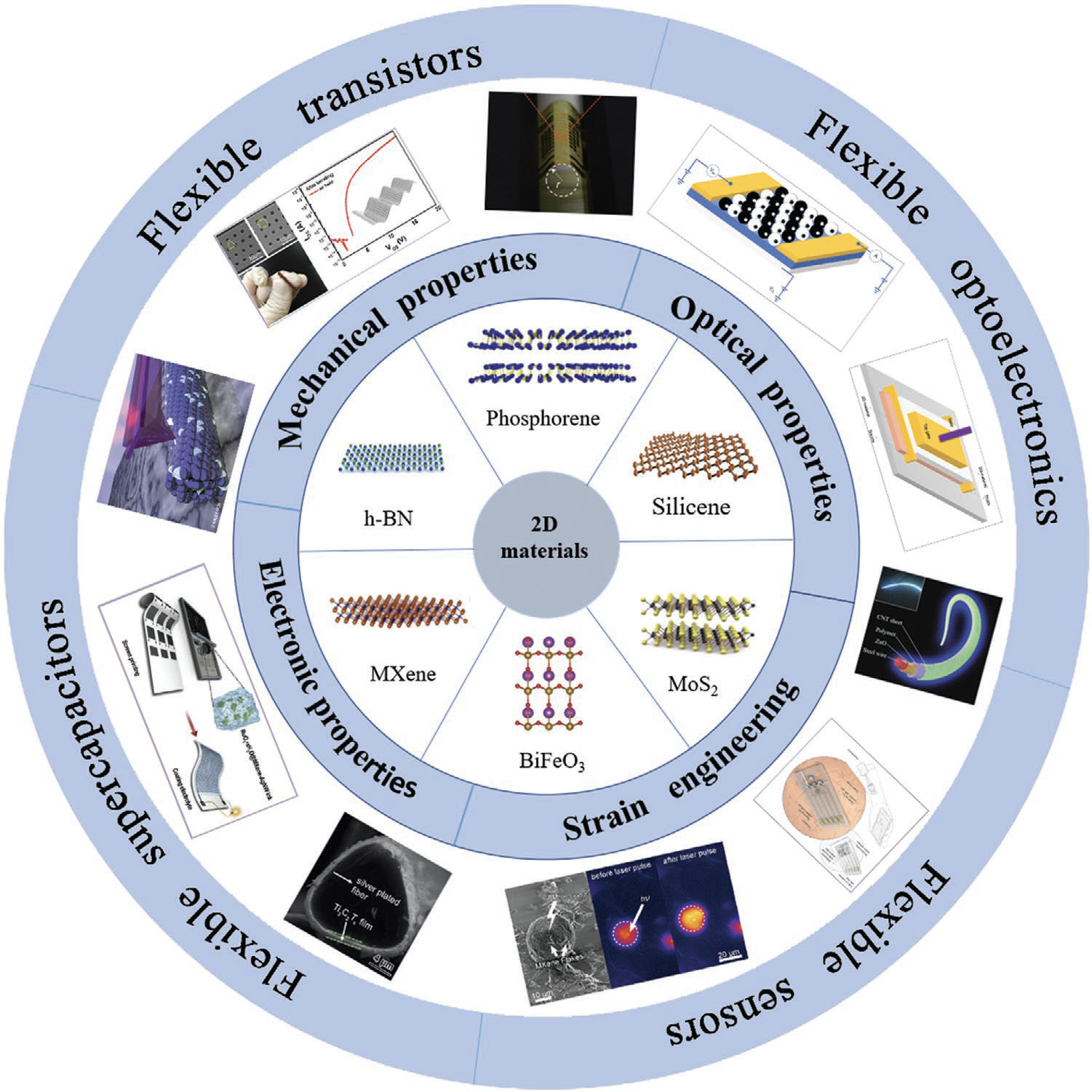 |
| Schematic illustration of the physical properties and applications of typically studied 2D materials. (Reprinted with permission by Wiley-VCH Verlag) |
| Due to excellent mechanical flexibility and compatibility with low-temperature manufacturing processes, 2D materials can be used in flexible electronic products with plastic substrates. Their use in flexible electronic products can overcome several technical challenges in systems based on traditional materials, such as low mobility, high driving voltage of organic materials, complex technological processes, and large leakage current of polycrystalline Si. |
| Furthermore, mechanical robustness and their atomic thickness provide 2D materials with high transparency in the visible range and makes them suitable for flexible, transparent electronic devices that are subject to mechanical strain and cyclic stress. |
| A recent review paper in Small ("Flexible 2D Materials beyond Graphene: Synthesis, Properties, and Applications") takes an in-depth look at the properties and preparation methods for 2D materials beyond graphene and their applications in flexible devices. |
| Different 2D materials show different physical properties (see table below) for specific applications in flexible devices, such as flexible transistors, optoelectronics, sensors, and supercapacitors. |
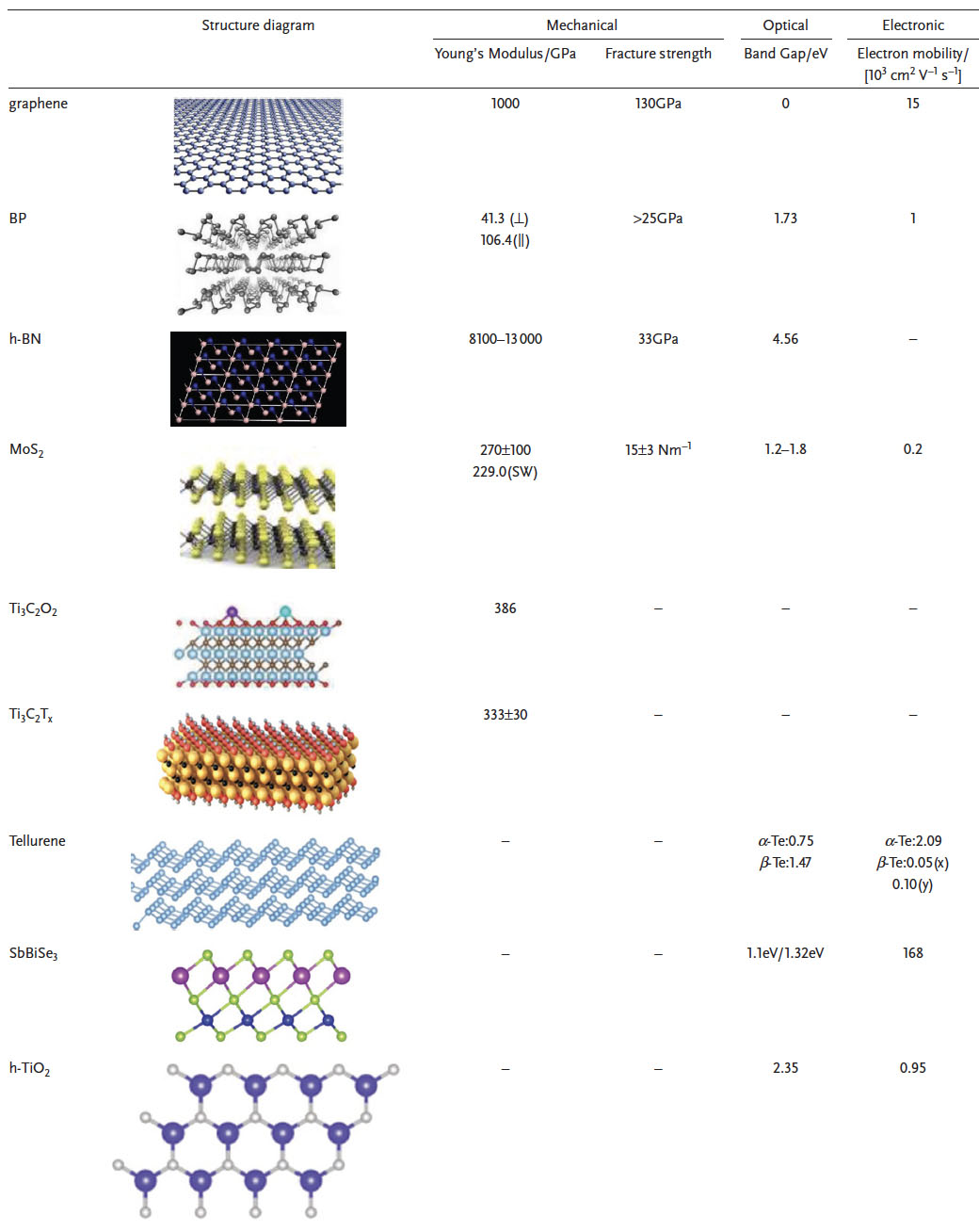 |
| Physical properties of 2D semiconductors. (Reprinted with permission by Wiley-VCH Verlag) (click on image to enlarge) |
| Fabrication techniques of 2D materials, which include top-down and bottom-up methods, have become mature and the various preparation and transfer methods are suitable for different 2D materials with many specific requirements, for example, mass production, large film or clean surface, and so on, acting as the main functional layer for versatile devices. |
| Top-down methods are suitable for materials with a layered structure of bulk materials. By applying an external shearing force on the material body, the distance between the layers is enlarged to weaken the van der Waals force between layers, thereby peeling off the 2D crystals. This type of method is usually suitable for layered 2D materials, and its common feature is to start with bulk or powdered materials, and use some technique to strip the 2D materials of multiple layers to obtain a few layers or monolayer 2D materials. The methods mainly include: mechanical exfoliation method, liquid exfoliation method, electrochemical exfoliation method, and ball milling method. |
| Bottom-up methods show good compatibility with a wide range of applications benefiting from the diversity in principle. It mainly includes magnetron sputtering, chemical vapor deposition (CVD), and wet chemical methods. |
| Once produced, the 2D materials need to be assembled for device creation. To that end, they need to be transfered from their production process to the assembly process by wet transfer, dry transfer, and vacuum transfer. |
| Generally, flexible devices based on 2D materials have made some preliminary progress in the applications of flexible thin-film transistors, solar cells, sensors, and supercapacitors. |
| The authors conclude their review by emphasizing that more fundamental research is required for both synthesis and devices of 2D materials. The CVD-synthesized graphene, h-BN, or TMDs have already succeeded in large-area and high-uniformity, but the crystal quality is still limited by the defects and small grain boundaries. |
| Furthermore, the subsequent transfer process often causes the contamination of the material, which can deteriorate the crystal quality. That makes the controllable synthesis of large-area 2D materials with high-quality and contamination-free transfer method a research priority of developing flexible 2D devices. |
| In addition, the integration of different functional flexible devices is the most challenging topic for future research. For now, most of the functional flexible devices, such as transistors, sensors, solar cells, and supercapacitors, have been well demonstrated as individual devices. However, the cross-working and integration of these devices into one overall device are pivotal for practical applications. |
 By
Michael
Berger
– Michael is author of four books by the Royal Society of Chemistry:
Nano-Society: Pushing the Boundaries of Technology (2009),
Nanotechnology: The Future is Tiny (2016),
Nanoengineering: The Skills and Tools Making Technology Invisible (2019), and
Waste not! How Nanotechnologies Can Increase Efficiencies Throughout Society (2025)
Copyright ©
Nanowerk LLC
By
Michael
Berger
– Michael is author of four books by the Royal Society of Chemistry:
Nano-Society: Pushing the Boundaries of Technology (2009),
Nanotechnology: The Future is Tiny (2016),
Nanoengineering: The Skills and Tools Making Technology Invisible (2019), and
Waste not! How Nanotechnologies Can Increase Efficiencies Throughout Society (2025)
Copyright ©
Nanowerk LLC
|

Become a Spotlight guest author! Join our large and growing group of guest contributors. Have you just published a scientific paper or have other exciting developments to share with the nanotechnology community? Here is how to publish on nanowerk.com. |
