| Aug 11, 2023 |
New technique enables precise atomic-scale manufacturing using electron beams |
| (Nanowerk Spotlight) Researchers have developed a novel technique that combines two approaches to nanofabrication - top-down and bottom-up methods - to enable unprecedented atomic-scale precision manufacturing using a focused electron beam. |
| Their work has been published in Advanced Materials ("Top-Down Fabrication of Atomic Patterns in Twisted Bilayer Graphene"). |
| Top-down methods, such as lithography, employ external influences to modify materials. While they offer precision patterning, their resolution is often constrained by factors like beam size and scattering effects. On the other hand, bottom-up methods capitalize on the spontaneous self-assembly of atoms and molecules through chemical reactions, granting atomic-level control. However, the positioning in this method tends to be random rather than directed. |
| The novel technique demonstrated on twisted bilayer graphene (TBG) harmoniously integrates these two approaches. Here's how it works: The focused electron beam provides the top-down control, pinpointing exact positions. Concurrently, heating the sample triggers the bottom-up self-assembly of atoms, specifically at the defect sites created by the beam. |
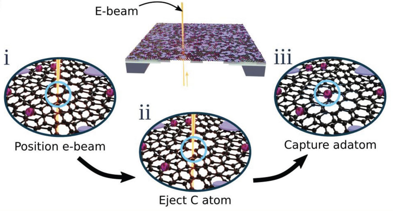 |
| Conceptual workflow for attaching diffusing adatoms to TBG involving i) positioning the e-beam at the location of interest, ii) ejection of a carbon atom, and iii) spontaneous capture of an adatom at the defect site. (Reprinted with permission from Wiley-VCH Verlag) |
| The pivotal breakthrough lies in the use of the tightly focused electron beam to eject carbon atoms from specific locations in the TBG lattice through a process known as direct knock-on. This action creates vacancies in the lattice, which then become attachment sites for foreign atoms. |
| Supporting the TBG sample on a heater chip, researchers evaporate source material onto its surface. By raising the temperature, they can cleanse contaminants and encourage adatom migration across the surface. This also regulates vacancy diffusion rates within the lattice. An ingenious automated feedback control system then detects when these vacancies are occupied, enabling the reproduction of arbitrary atom patterns by adeptly controlling the electron beam's positioning. |
| Dr. Stephen Jesse from the Center for Nanophase Materials Sciences at Oak Ridge National Laboratory, the lead author of the study, emphasized the significance of this innovation: “This merging of top-down beam control with bottom-up atomic self-assembly represents a major advancement in nanofabrication. We’ve showcased that intricate atom-by-atom structures can now be crafted in a reproducible, automated manner, a feat previously deemed unattainable.” |
| A crucial component in this process is the extremely thin TBG membrane, which offers unparalleled control over the electron beam's size and position. The researchers also highlighted the potential to refine the technique further by independently controlling the temperatures of the TBG and source material. |
| In their experiments, the team successfully patterned both copper and chromium dopants into intricate shapes with sub-nanometer precision across multiple sessions. They employed High-angle annular dark field (HAADF) imaging to distinguish between the atomic species based on their intensity. This innovative approach holds promise for other 2D materials and elements, heralding a new era for single-atom electronics, sensors, and quantum information applications. |
| Reflecting on the broader implications, Dr. Jesse remarked, “This holds transformative potential for the continued miniaturization of electronic devices and precision manufacturing. As we refine this technique, we foresee a future where machine-learning aids in the atom-by-atom design of materials, tailoring them for bespoke properties and functionalities.” |
| In essence, this pioneering fabrication method marries the precision of top-down lithography with the atomic specificity inherent in bottom-up self-assembly. Such a union could very well catalyze a thrilling new epoch of atomic-scale manufacturing. |
 By
Michael
Berger
– Michael is author of four books by the Royal Society of Chemistry:
Nano-Society: Pushing the Boundaries of Technology (2009),
Nanotechnology: The Future is Tiny (2016),
Nanoengineering: The Skills and Tools Making Technology Invisible (2019), and
Waste not! How Nanotechnologies Can Increase Efficiencies Throughout Society (2025)
Copyright ©
Nanowerk LLC
By
Michael
Berger
– Michael is author of four books by the Royal Society of Chemistry:
Nano-Society: Pushing the Boundaries of Technology (2009),
Nanotechnology: The Future is Tiny (2016),
Nanoengineering: The Skills and Tools Making Technology Invisible (2019), and
Waste not! How Nanotechnologies Can Increase Efficiencies Throughout Society (2025)
Copyright ©
Nanowerk LLC
|

Become a Spotlight guest author! Join our large and growing group of guest contributors. Have you just published a scientific paper or have other exciting developments to share with the nanotechnology community? Here is how to publish on nanowerk.com. |
