| Dec 13, 2023 |
The unmatched potential of perovskite LEDs as candidates for next-generation displays |
| (Nanowerk Spotlight) Metal-halide perovskites represent an emerging class of low-cost semiconductors with promising light-emitting capabilities that could enable the next generation of vibrant, energy-efficient displays. However, difficulties in fabrication, efficiency, and stability have obstructed the path towards commercialization of perovskite LEDs (PeLEDs). Without solving these lingering challenges from years of R&D, PeLEDs seemed fated to languish as lab demonstrations. |
| But now, new research integrating perovskite films with two-dimensional electronics finally provides manufacturing solutions. Capitalizing on these advances in materials and fabrication, researchers from Yonsei and Korea Universities developed centimeter-scale integrated PeLED displays achieving key metrics on par or better than existing standards. This breakthrough work suggests the long-awaited transition of PeLEDs from lab concept to next-generation commercial displays could soon occur. |
| The team has published their findings in Advanced Materials ("Perovskite Light-Emitting Diode Display Based on MoS2 Backplane Thin-Film Transistors"). |
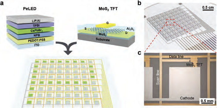 |
| The device structure of active-matrix PeLED display using MoS2 backplane TFT. a) Schematic illustration of a CsPbBr3 PeLED display integrated with a MoS2 TFT-based backplane. b) Optical image of an active-matrix PeLED display fabricated on a glass substrate. c) Magnified optical image showing the structure of the display. (Reprinted with permission from Wiley-VCH) |
| Adjacent advancements in two-dimensional (2D) transition metal dichalcogenides (TMDCs) like molybdenum disulfide (MoS2) have also enabled critical progress. With their atomic thickness, high charge carrier mobility, and capability for flexible low-temperature fabrication, TMDCs show potential as integrated control circuitry to drive PeLED displays. |
| Capitalizing on these breakthroughs, a new study from Yonsei and Korea Universities integrated PeLED pixels with MoS2 transistor arrays to create full active matrix displays with superior performance. Refinements included using single-source thermal evaporation to deposit exceptionally uniform CsPbBr3 perovskite layers across 49 cm2 areas and implementing MoS2 thin-film transistors (TFTs) as robust low-power backplanes to actively address the LED pixels. |
| Compared to previous small-scale demonstrations, this heterogeneous integration of emergent nanomaterials yielded 8x8 centimeter-scale displays with one millisecond response times, no visible crosstalk between pixels, and brightness control spanning three orders of magnitude. The evaporated perovskite films also showed impressive stability, with lifetimes over an hour even without encapsulation. |
| Remarkably, the simple single-source evaporation process achieved equivalent or better LED characteristics compared to more complex techniques, while also ensuring the film reliability necessary for electronic displays. This addresses a key manufacturing challenge that has restrained commercial progress. Enabled by these innovations, the prototypes compare favorably with existing display technologies in metrics like color purity, brightness, and switching speed. |
| By combining the advantages of TMDC circuits and PeLED emitters into full integrated systems, this research provides a blueprint toward next-generation displays. The advances demonstrate the potential for perovskites to move out of the lab into tomorrow’s flexible displays, monitors, and televisions. Looking forward, the heterogeneous integration paradigm could also inspire hybrid technologies blending other 2D materials or quantum dots with perovskite’s useful optoelectronic properties. |
| With many historical obstacles to real-world PeLED adoption now elegantly overcome through material and fabrication optimizations, this technology finally appears poised for commercial development pending incremental improvements. Mainstream perovskite displays could reach widespread usage within just a few years, bringing lower costs along with excellent color quality and diminished environmental impacts compared to existing standards. |
 By
Michael
Berger
– Michael is author of four books by the Royal Society of Chemistry:
Nano-Society: Pushing the Boundaries of Technology (2009),
Nanotechnology: The Future is Tiny (2016),
Nanoengineering: The Skills and Tools Making Technology Invisible (2019), and
Waste not! How Nanotechnologies Can Increase Efficiencies Throughout Society (2025)
Copyright ©
Nanowerk LLC
By
Michael
Berger
– Michael is author of four books by the Royal Society of Chemistry:
Nano-Society: Pushing the Boundaries of Technology (2009),
Nanotechnology: The Future is Tiny (2016),
Nanoengineering: The Skills and Tools Making Technology Invisible (2019), and
Waste not! How Nanotechnologies Can Increase Efficiencies Throughout Society (2025)
Copyright ©
Nanowerk LLC
|

Become a Spotlight guest author! Join our large and growing group of guest contributors. Have you just published a scientific paper or have other exciting developments to share with the nanotechnology community? Here is how to publish on nanowerk.com. |
