| Jan 19, 2024 |
Ultra-thin 2D crystal poised to unlock faster, lower power electronics |
| (Nanowerk Spotlight) For over 50 years, the electronics industry has consistently delivered exponential increases in computing power, as predicted by Moore's Law. This trend of constant enhancement has been enabled by the perpetual miniaturization of silicon transistors. However, scientists have long foreseen an approaching limit, as shrinking conventional silicon devices leads to problematic quantum effects like current leakage. |
| Researchers have proposed integrating emerging two-dimensional (2D) materials like molybdenum disulfide (MoS2) as transistor channels. Their atomically thin structure could enable further miniaturization. 2D materials get their name from having thickness on the nanometer scale, sometimes even approaching a single layer of atoms. Yet a lingering obstacle has been the lack of an appropriately thin dielectric material to separate the gate and channel. Without a quality insulator up to the task, transistors cannot function properly. |
| Without a quality insulator up to the task, transistors cannot function properly. The rare stacks exhibiting sufficient performance relied on flimsy organic layers unfit for mass production and commercial integration. Sturdy, scalable dielectrics with smooth surfaces free of defects have remained elusive. |
| Now a team of scientists from China’s Wuhan University and Nanjing University have realized ultrathin high-quality lanthanum oxychloride crystals using a novel chemical vapor deposition technique. |
| Published in Advanced Materials ("Ultrathin Van der Waals Lanthanum Oxychloride Dielectric for 2D Field-Effect Transistors"), their work demonstrates exceptional dielectric properties meeting and exceeding industry metrics. Integrated MoS2 field effect transistors with the lanthanum oxychloride dielectrics as gates exhibit remarkable switching characteristics and negligible hysteresis. The researchers attribute such functionality to the material's intrinsic lack of dangling bonds, which enables clean van der Waals bonding with the layered semiconductor. |
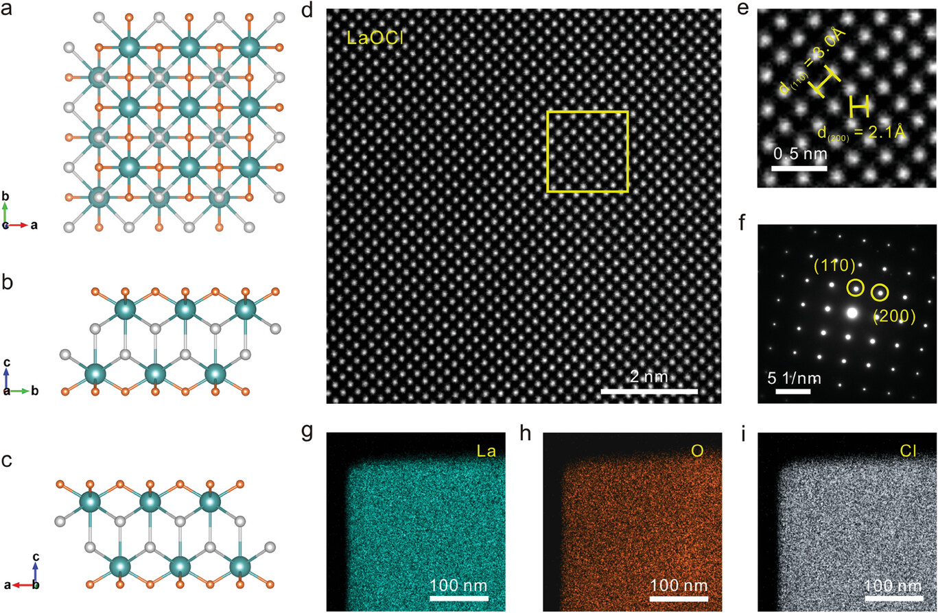 |
| Atomic structure of ultrathin vdW LaOCl single crystals. a−c) Crystal structure of ultrathin LaOCl nanosheet along the c-axis, a-axis, and b-axis. d−f) HAADF-STEM, and SAED of an ultrathin vdW LaOCl single crystal. The magnified STEM image in (e) is from the yellow box region in (d). g−i) EDS elemental mapping of an ultrathin vdW LaOCl nanosheet. (Reprinted with permission by Wiley-VCH Verlag) |
| The most common gate dielectric is silicon dioxide, known generally as glass, owing to its amorphous structure. Though abundant and readily deposited, SiO2 features a modest dielectric constant, limiting its ultimate thinness and therefore the channel length of transistors it can isolate. |
| More recently, the industry has adopted hafnium-based isolators like HfO2 to allow for smaller gates. However, their innate structural disorder gives rise to dangling bonds, trapped charges, and surface roughness that degrade device performance and reliability. |
| 2D materials have gained attention for their potential to continue historical scaling trends once silicon nears its physical limits. Their layered crystalline structure lacks out-of-plane dangling bonds and can conform intimately with adjacent strata. |
| However, identifying a suitable insulator that bonds well to semiconductors like MoS2 without ruining their pristine electronic properties has remained an unsolved quandary. Researchers have only achieved high-performing prototypes by relying on polymer separators which cannot survive manufacturing environments or match the consistency of traditional oxide films. |
| Lanthanum oxychloride distinguishes itself with a wide bandgap exceeding 4 eV and towering dielectric constant over 10, translating to excellent insulating capability in nanometer-thin sheets. |
| For comparison, workhorse silicon dioxide has a modest dielectric constant around 4, while higher-performance hafnia films still top out under 30. The sizable discrepancy directly enables lanthanum oxychloride layers to better concentrate electric fields using less material. And even minute current leakage through an ultrahigh-K gate stack may corrupt integrated logic or memory. Lanthanum oxychloride's substantially widened bandgap consequently blocks more tunneling electrons. |
| Additionally, The anisotropic crystals also inherently terminate with complete LaCl3 layers, rendering dangling bond-free surfaces. Dangling bonds are incomplete molecular connections that degrade material performance and reliability. Together with the material’s straightforward exfoliation and stacking, these characteristics hinted at ideal integration with 2D channel materials, spurring investigation into synthesis techniques. |
| Together with the material’s straightforward exfoliation and stacking, these characteristics hinted at ideal integration with 2D channel materials, spurring investigation into synthesis techniques. |
| The researchers’ custom low-pressure vapor deposition procedure using LaCl3 and La2O3 precursors allows precision control over lanthanum oxychloride nucleation and growth kinetics. Regulating the deposited film’s thickness, they produced samples as thin as 1.3 nm, comprising just two molecular layers. |
| Subsequent atomic force and transmission electron microscopy verified a pristine, highly ordered structure almost completely devoid of defects. X-ray photoelectron spectroscopy and diffraction confirm the proper elemental composition and bonding within the material. |
| To characterize the dielectric properties experimentally, the team first constructed metal-insulator-metal capacitor structures featuring lanthanum oxychloride. Electrical probing returned an exceptional dielectric constant of 10.8 along with outstanding insulating performance quantified by miniscule leakage current. This low conductivity trounces typical figures for both conventional silicon dioxide and previous best-in-class experimental dielectrics like boron nitride. Measuring extremely high breakdown field strengths exceeding 10 MV/cm further proves the viability for nanoelectronics applications demanding ultrathin, flawless films. |
| Integrating their vapor-grown crystals as top-gate dielectrics onto exfoliated molybdenum disulfide yielded transistors switching on and off over four orders of magnitude, competitive with state-of-the-art demonstrations but relying on a deposition-compatible insulator stack. |
| Low hysteresis values down to nearly zero observed upon sweeping gate voltage verifies suppression of charge trapping often plaguing devices with imperfect interfaces. Hysteresis refers to variation in the electronic state or output value depending on whether voltage is ramped up or down. Negligible variation between backward and forward characteristics signifies stability amenable to digital logic. |
| Negligible variation between backward and forward characteristics signifies stability amenable to digital logic. Simulation and spectroscopy results confirm a wide bandgap MoS2 layer electronically isolated from the overlaying interconnects and substrate influences that can interfere with transport. |
| The researchers attribute such excellent functionality to robust van der Waals bonding between the layered materials, producing an atomically sharp junction without disorder. |
| Ongoing transistor scaling has enabled exponential computing performance gains for decades in accordance with Moore’s Law projections. While silicon still has legs in the near future thanks to novel architectures, materials like two-dimensional semiconductors and atomically flat dielectrics will become essential for advancement within this decade. |
| Demonstrating the immense promise of lanthanum oxychloride films with properties superior to conventional insulators, this research opens the door to next-generation electronics relying on layered van der Waals stacking. |
| Compatibility with existing foundry processes and environments provides a path for rapid manufacturing scale-up. By addressing previous roadblocks, the depressingly elusive goal of faster, smaller, cheaper computing now seems achievable through hybrid material integration. |
 By
Michael
Berger
– Michael is author of four books by the Royal Society of Chemistry:
Nano-Society: Pushing the Boundaries of Technology (2009),
Nanotechnology: The Future is Tiny (2016),
Nanoengineering: The Skills and Tools Making Technology Invisible (2019), and
Waste not! How Nanotechnologies Can Increase Efficiencies Throughout Society (2025)
Copyright ©
Nanowerk LLC
By
Michael
Berger
– Michael is author of four books by the Royal Society of Chemistry:
Nano-Society: Pushing the Boundaries of Technology (2009),
Nanotechnology: The Future is Tiny (2016),
Nanoengineering: The Skills and Tools Making Technology Invisible (2019), and
Waste not! How Nanotechnologies Can Increase Efficiencies Throughout Society (2025)
Copyright ©
Nanowerk LLC
|

Become a Spotlight guest author! Join our large and growing group of guest contributors. Have you just published a scientific paper or have other exciting developments to share with the nanotechnology community? Here is how to publish on nanowerk.com. |
